
Hardware manual


Rev. 3.0, 09/98, page 188 of 361
TDR-empty, TSR-empty, receive-end, and receive-error interrupts are requested
independently.
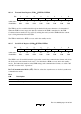
10.1.2 Block Diagram
Figure 10.1 shows a block diagram of one serial communication interface channel.
RDR
RXD
TXD
SCK
TDR
RSR TSR
SSR
SCR
SMR
Communication
control
Baud rate
generator
Internal
data bus
Internal
clock
RDR
RSR
TDR
TSR
SSR
SCR
SMR
BRR
Legend:
: Receive Shift Register (8 bits)
: Receive Data Register (8 bits)
: Transmit Shift Register (8 bits)
: Transmit Data Register (8 bits)
: Serial Mode Register (8 bits)
: Serial Control Register (8 bits)
: Serial Status Register (8 bits)
: Bit Rate Register (8 bits)
Module data bus
Ø
Ø/4
Ø/16
Ø/64
External clock source
Clock
Parity
generate
Parity check
Interrupt signals
TEI
TXI
RXI
ERI
BRR
Bus interface
Figure 10.1 Block Diagram of Serial Communication Interface
10.1.3 Input and Output Pins
Table 10.1 lists the input and output pins used by the SCI module.