
Hardware manual


Rev. 3.0, 09/98, page 185 of 361
9.3.2 PWM Operation
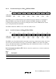
Figure 9.3 is a timing chart of the PWM operation.
N(a) H' 00 (b) H' 01 H' 02 H' F9 (d) H' 00 H' 01
N
H' FF
(d) M
N – 1 N + 1
(C)
(C)(b)(a)
(e)
TCNT
clock pulses
OE
Ø
TCNT
DTR
( OS = “0” )
PWM output
N written in DTR
PWM 1 cycle
( OS = “1” )
M written in DTR
Note: * Used for port 4 input/output: state depends on values in data register and data direction register.
Figure 9.3 PWM Timing
(1) Positive Logic (OS = “0”)
①① When (OE = “0”) − (a) in Figure 9.3: The timer count is held at H'00 and PWM output is
inhibited. [Pin 4
6
(for PW0) or pin 4
7
(for PW1) is used for port 4 input/output, and its state
depends on the corresponding port 4 data register and data direction register.] Any value (such as
N in figure 9.3) written in the DTR becomes valid immediately.
②② When (OE = “1”)
i) The timer counter begins incrementing. The PWM output goes High when TCNT changes
from H'00 to H'01, unless DTR = H'00. [(b) in figure 9.3]
ii) When the count passes the DTR value, the PWM output goes Low. [(c) in figure 9.3]