
Hardware manual


Rev. 3.0, 09/98, page 150 of 361
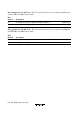
If the upper byte of ICRA/B/C/D is being read when the corresponding input capture signal
arrives, the internal input capture signal is delayed by one state. Figure 7.11 shows the timing for
this case.
Ø
Input at
FTIA pin
Internal input
capture signal
T
1
T
2
T
3
Read cycle: CPU reads upper byte of ICRA or ICRC
Figure 7.11 Input Capture Timing (1-State delay)
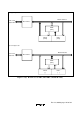
In buffer mode, this delay occurs if the CPU is reading either of the two registers concerned.
When ICRA and ICRC are used in buffer mode, for example, if the upper byte of either ICRA or
ICRC is being read when the FTIA input arrives, the internal input capture signal is delayed by
one state. Figure 7.12 shows the timing for this case. The case of ICRB and ICRD is similar.
FRC
ICFA to D
ICRA to D
Ø
Internal input
capture signal
N
N
Figure 7.12 Input Capture Timing (1-State delay, buffer mode)