
Hardware manual


Rev. 3.0, 09/98, page 149 of 361
(3) FRC Clear Timing: If the CCLRA bit in the TCSR is set to “1,” the FRC is cleared when
compare-match A occurs. Figure 7.9 shows the timing of this operation.
Ø
Internal input
capture signal
Input at FTI pin
Read cycle: CPU reads upper byte of ICR
T
1
T
2
T
3
Figure 7.9 Clearing of FRC by Compare-Match A
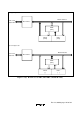
7.4.3 Input Capture Timing
(1) Input Capture Timing: An internal input capture signal is generated from the rising or
falling edge of the signal at the input capture pin FTIx (x = A, B, C, D), as selected by the
corresponding IEDGx bit in TCR. Figure 7.10 shows the usual input capture timing when the
rising edge is selected (IEDGx = “1”).
N
n
N + 1n + 1
n
n
M
N
M
Mm
n
FTIA
Ø
Internal input
capture signal
ICRA
FRC
ICRC
Figure 7.10 Input Capture Timing (Usual case)