
Emulation Probe User's Manual
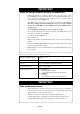
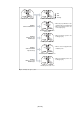
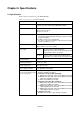
Table Of Contents
- Preface
- Contents
- 1. Precautions for Safety
- 2. Preparation
- 3. Setting Up
- 3.1 Selecting Clock Supply
- 3.2 Using an Internal Oscillator Circuit Board
- 3.3 Using the Oscillator Circuit on the Target System
- 3.4 Using the Internal Oscillator Circuit
- 3.5 Setting Switches
- 3.6 A-D Conversion Bypass Capacitor
- 3.7 Connecting the PC7501
- 3.8 Connecting the Target System
- (1) Connecting to a 100-pin LCC Socket
- (2) Connecting to a 100-pin 0.65-mm-pitch Foot Pattern (Part 1)
- (3) Connecting to a 100-pin 0.65-mm-pitch Foot Pattern (Part 2)
- (4) Connecting to a 100-pin 0.65-mm-pitch Foot Pattern (Part 3)
- (5) Connecting to a 100-pin 0.5-mm-pitch Foot Pattern (Part 1)
- (6) Connecting to a 100-pin 0.5-mm-pitch Foot Pattern (Part 2)
- (7) Connecting to a 100-pin 0.5-mm-pitch Foot Pattern (Part 3)
- (8) Connecting to a 144-pin 0.5-mm-pitch Foot Pattern
- 4. Usage
- 5. Specifications
- 6. Troubleshooting
- 7. Maintenance and Guarantee
( 59 / 76 )
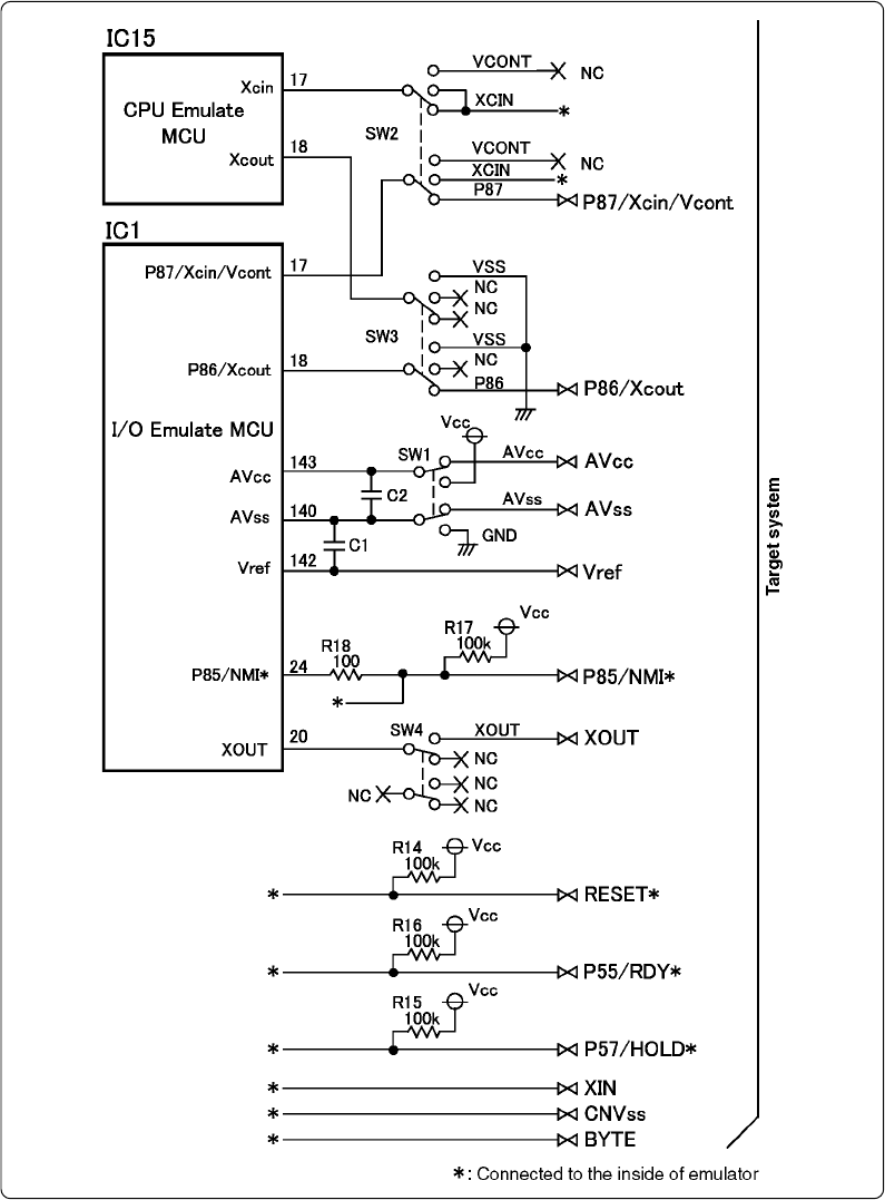
Figure 5.1 Connection diagram (1/2)
5.2 Connection Diagrams
Figures 5.1 and 5.2 show the connection diagrams of the M30850T-EPB. These connection diagrams
mainly show the interface section. The signals not shown in Figures 5.1 and 5.2 are connected to the
evaluation MCU in the emulation probe and the target system directly. The circuits not connected to
the target system such as the emulator's control system are omitted.
Table 5.2 lists the electrical characteristics of the IC used for the user interface. Refer to it when using
the emulator.