
Emulation Probe User's Manual
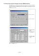
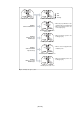
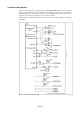
Table Of Contents
- Preface
- Contents
- 1. Precautions for Safety
- 2. Preparation
- 3. Setting Up
- 3.1 Selecting Clock Supply
- 3.2 Using an Internal Oscillator Circuit Board
- 3.3 Using the Oscillator Circuit on the Target System
- 3.4 Using the Internal Oscillator Circuit
- 3.5 Setting Switches
- 3.6 A-D Conversion Bypass Capacitor
- 3.7 Connecting the PC7501
- 3.8 Connecting the Target System
- (1) Connecting to a 100-pin LCC Socket
- (2) Connecting to a 100-pin 0.65-mm-pitch Foot Pattern (Part 1)
- (3) Connecting to a 100-pin 0.65-mm-pitch Foot Pattern (Part 2)
- (4) Connecting to a 100-pin 0.65-mm-pitch Foot Pattern (Part 3)
- (5) Connecting to a 100-pin 0.5-mm-pitch Foot Pattern (Part 1)
- (6) Connecting to a 100-pin 0.5-mm-pitch Foot Pattern (Part 2)
- (7) Connecting to a 100-pin 0.5-mm-pitch Foot Pattern (Part 3)
- (8) Connecting to a 144-pin 0.5-mm-pitch Foot Pattern
- 4. Usage
- 5. Specifications
- 6. Troubleshooting
- 7. Maintenance and Guarantee

( 51 / 76 )
4.3 Starting Up the Emulator Debugger (Setting the EMEM Dialog Box)
The EMEM dialog box will appear after setting the Init dialog box by starting up the emulator
debugger or completing downloading the firmware. Here explains how to set a processor mode of
the target MCU, allocate the emulation memory and set the emulator work area. Figure 4.3 shows the
EMEM dialog box display.
Figure 4.3 EMEM dialog box
1.Debug monitor bank
address
2. Processor mode
3.Allocation of the
internal ROM area
5.Levels of each pin
4. Allocations of the
expansion emulation
memory