
Emulation Probe User's Manual

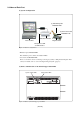
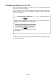

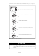
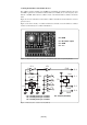
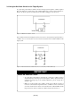
Table Of Contents
- Preface
- Contents
- 1. Precautions for Safety
- 2. Preparation
- 3. Setting Up
- 3.1 Selecting Clock Supply
- 3.2 Using an Internal Oscillator Circuit Board
- 3.3 Using the Oscillator Circuit on the Target System
- 3.4 Using the Internal Oscillator Circuit
- 3.5 Setting Switches
- 3.6 A-D Conversion Bypass Capacitor
- 3.7 Connecting the PC7501
- 3.8 Connecting the Target System
- (1) Connecting to a 100-pin LCC Socket
- (2) Connecting to a 100-pin 0.65-mm-pitch Foot Pattern (Part 1)
- (3) Connecting to a 100-pin 0.65-mm-pitch Foot Pattern (Part 2)
- (4) Connecting to a 100-pin 0.65-mm-pitch Foot Pattern (Part 3)
- (5) Connecting to a 100-pin 0.5-mm-pitch Foot Pattern (Part 1)
- (6) Connecting to a 100-pin 0.5-mm-pitch Foot Pattern (Part 2)
- (7) Connecting to a 100-pin 0.5-mm-pitch Foot Pattern (Part 3)
- (8) Connecting to a 144-pin 0.5-mm-pitch Foot Pattern
- 4. Usage
- 5. Specifications
- 6. Troubleshooting
- 7. Maintenance and Guarantee
( 27 / 76 )
3.2 Using an Internal Oscillator Circuit Board
(1) Kinds of Oscillator Circuit Boards
The PC7501 comes with an oscillator circuit board OSC-3 (30 MHz). And an oscillator circuit board
OSC-3 (32 MHz) is included with this product. If you use the internal oscillator circuit board of the
PC7501 as a main clock, choose "Internal" in the emulator debugger after replacing oscillator circuit
boards to change a clock supplied to an MCU.
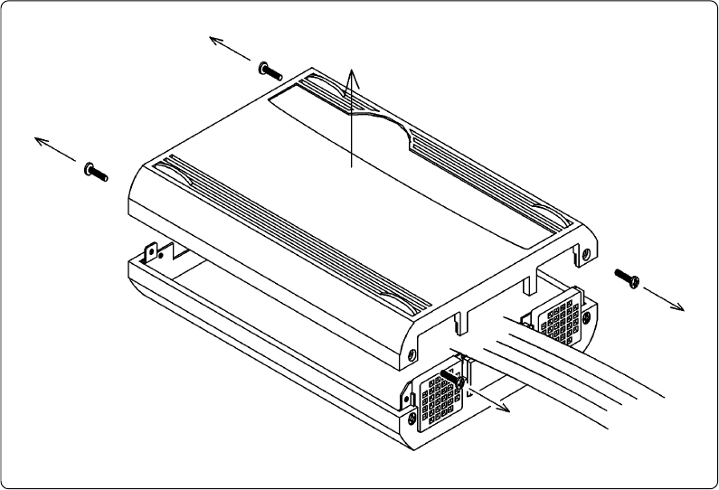
(2) Replacing an Oscillator Circuit Board
1. Remove the four screws of both sides of this product and lift off the upper cover (see Figure 3.1).
Figure 3.1 Removing the upper cover