M30830T-EPB Emulation Pod for M32C/81, 82 and 83 Groups User's Manual Rev.2.
* IIC61-1004-051 is a trademark of Yamaichi Electronics Co., Ltd. * NQPACK, YQPACK, YQSOCKET, YQ-Guide, HQPACK, TQPACK and TQSOCKET are trademarks of Tokyo Eletech Corporation. Keep safety first in your circuit designs! • Renesas Technology Corporation and Renesas Solutions Corporation put the maximum effort into making semiconductor products better and more reliable, but there is always the possibility that trouble may occur with them.
Preface The M30830T-EPB is an emulation probe for M32C/81, 82 and 83 Groups of Renesas MCUs. The M30830T-EPB is used by connecting to the PC7501 emulator main unit. This user's manual mainly describes specifications of the M30830T-EPB emulation probe and how to setup it. For details on the following products, which are used with the M30830T-EPB, refer to each product's user's manual.
Contents Chapter 1. Precautions for Safety .......................................................................................... 7 1.1 Safety Symbols and Meanings ............................................................................. 9 Chapter 2. Preparation ......................................................................................................... 17 2.1 Terminology ....................................................................................................... 18 2.
4.3 Starting Up the Emulator Debugger (Setting EMEM Dialog Box) ................... 47 (1) Setting the Debug Monitor Bank Address ............................................... 48 (2) Selecting the Processor Mode .................................................................. 48 (3) Setting the Emulation Memory ................................................................ 49 (4) Emulation Memory Allocation as Expansion Area ................................. 49 (5) Referring MCU STATUS ...............
MEMO ( 6 / 72 )
Chapter 1. Precautions for Safety This chapter describes precautions for using this product safely and properly. For precautions for the emulator main unit and the emulator debugger, refer to each user's manual included with your product. 1.1 Safety Symbols and Meanings ..................................................................................................... 9 WARNING Warning for Handling This Product ..........................................................................
Note on Downloading Programs ................................................................................ 16 Note on On-chip Oscillator ........................................................................................ 16 Note on PLL Clock .................................................................................................... 16 Notes on Address-Match Interrupt............................................................................. 16 Note on Operating Frequency .................
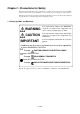
Chapter 1. Precautions for Safety In both the user's manual and on the product itself, several icons are used to insure proper handling of this product and also to prevent injuries to you or other persons, or damage to your properties. This chapter describes the precautions which should be taken in order to use this product safely and properly. Be sure to read this chapter before using this product. 1.
WARNING Warning for Handling This Product: • Do not disassemble or modify this product. Disassembling or modifying this product can cause damage. Warning for Installation: • Do not set this product in water or areas of high humidity. Spilling water or some other liquid into the main unit can cause an unrepairable damage. Warning for Use Environment: • This equipment is to be used in an environment with a maximum ambient temperature of 35°C. Care should be taken that this temperature is not exceeded.
IMPORTANT Notes on Downloading Firmware: • Before using this product for the first time, it is necessary to download the dedicated firmware (control software built into the PC7501). Please note that, to do this, it is necessary to start up the PC7501 in the maintenance mode. For firmware download procedures, see "4.2 Downloading Firmware" (page 46). Once the firmware has been downloaded, the product can be used by simply turning on the power. • Do not shut off the power while downloading the firmware.
IMPORTANT Note on NMI* Input: • NMI* input from the target system is accepted only while a user program is being executed (only while the RUN status LED on the PC7501's upper panel is lit). Notes on Interruption: • Even when the user program is not being executed (when the user program is paused or when runtime debugging is being performed), the evaluation MCU is operating for debugging purposes.
IMPORTANT Notes on Reset Vector Area: • For a reset vector area, memory of the emulator is always selected regardless of the setting of EMEM dialog. Therefore when setting the microprocessor mode, to use a ROM of the target system etc. as an area including a reset vector area, set a reset vector using a dump window etc. • The reset vector area can be changed only when a program is stopped. When a program is executed, the area can not be changed.
IMPORTANT Note on S/W Break: • S/W breaks generate break interruptions by forcibly inserting a BRK instruction "08h" instead of an instruction code. Therefore, when referencing the result of a trace in bus mode, "08h" is displayed for the instruction fetch address where a S/W break is set. Note on Differences between Actual MCU and Emulator: • Operations of the emulator differs from those of mask MCUs as listed below.
IMPORTANT Notes on A-D Input Selection Function: • To use A-D input group selection function, it is necessary to set the direction register of port P15 to input. Port 15 corresponds to the pin that performs A-D conversion. Example: To select A-D input for P00-P07, set the direction register of P150-P157 and P00-P07 to input. Also, when the port P0 group and port P2 group are selected for A-D input, port P15 cannot be used as an I/O port.
IMPORTANT Note on Downloading Programs: • When specifying a DRAM refresh interval, take note that when setting downloading a program to an internal ROM area and setting software breaks, the main clock operates in the divide-by-8 mode. Note on On-chip Oscillator: • Take note that you can not debug a program using the oscillation stop detection function (on-chip oscillator). If you use the function, be sure to evaluate a system with an actual MCU.
Chapter 2. Preparation This chapter describes the package components, the system configuration and the preparation for using this product for the first time. 2.1 Terminology ............................................................................................................................... 18 2.2 Package Components.................................................................................................................. 19 2.3 Other Tool Products Required for Development.................
Chapter 2. Preparation 2.1 Terminology Some specific words used in this user's manual are defined as follows: Emulator system This means an emulator system built around the PC7501 emulator. The PC7501 emulator system is configured with an emulator main unit, emulation probe, host machine and emulator debugger. Emulator main unit (Hereafter PC7501) This means an emulator main unit for M16C Family MCUs. Emulation probe This means the emulation probe (this product) for the M32C/81, 82 and 83 Group MCUs.
2.2 Package Components The M30830T-EPB package consists of the following items. When unpacking, check to see if your M30830T-EPB contains all of these items. Table 2.1 Package components Item Quantity M30830T-EPB emulation probe 1 M30800T-PTC converter board for 100-pin LCC 1 IC61-1004-051 100-pin LCC socket made by Yamaichi Electronics Co., Ltd.
2.4 Name of Each Part (1) System Configuration Emulator debugger M3T-PD308F (1) Emulation probe M30830T-EPB (2) Converter board M30800T-PTC Emulator PC7501 Host machine Target board LPT parallel, USB or LAN interface Figure 2.1 System configuration (1) Emulation probe (M30830T-EPB) This emulation probe contains an evaluation MCU. (2) Converter board (M30800T-PTC) This is a converter board for connecting to the target system (for 100-pin 0.65-mm-pitch LCC socket). For details, refer to "3.
(1) System Status LEDs The system status LEDs indicate the emulator PC7501's power supply, firmware operating status, etc. Table 2.3 lists the definition of each system status LED. Table 2.3 Definition of system status LEDs Name Status POWER ON Emulator system power supply is turned ON. OFF Emulator system power supply is turned OFF. ON Emulator system is operating normally. SAFE Flashing ERROR Meaning Specific mode (maintenance mode) for downloading the firmware.
2.5 When Using the Emulator for the First Time If you have purchased this emulation probe newly, it is necessary to download the firmware. The download procedure is given in Figure 2.3. Before downloading the firmware, check the emulator debugger is installed and the PC7501 is connected to the host machine. For more information, see each user's manual of the emulator debugger and the PC7501. Connect the PC7501 and this product.
Chapter 3. Setting Up This chapter describes switch settings required for using this product and how to connect this product to the PC7501 and the target system. 3.1 Removing the Upper Cover ........................................................................................................ 24 3.2 Selecting Clock Supply .............................................................................................................. 25 (1) Using the Oscillator Circuit on the Target System ................
Chapter 3. Setting Up To use this emulation probe with your target system, it is necessary to change the input frequency. Set the input frequency after removing the upper cover. 3.1 Removing the Upper Cover The procedure of removing the upper cover is shown below. (1) Remove the four screws of both sides of this product and lift off the upper cover (see Figure 3.1). (2) Change the input frequency following the procedure. (3) Replace the upper cover and secure the four screws. Figure 3.
3.2 Selecting Clock Supply There are two ways to supply a clock to the MCU, using the oscillator circuit of the emulator or using the oscillator circuit on the target system. Table 3.1 lists the factory-settings of each clock supply. Table 3.1 Clock supply to the MCU Clock Description Display of emulator debugger Default setting Internal oscillator circuit of emulator (OSC-3: 30 MHz) Internal Yes Target system External - Internal oscillator circuit of emulator (OSC-2: 32.
(1) Using the Oscillator Circuit on the Target System When turning on the power supply, the internal clock of emulator is selected to supply the clock to the MCU. To use the external clock on the target system, change the clock by the Init dialog box when starting up the emulator debugger or the CLK command on the script window (For details, refer to the user's manual of the emulator debugger). Figure 3.2 External oscillator circuit Figure 3.
(2) Changing the Internal Oscillator Circuit of the Emulator An oscillator circuit board (OSC-3) for 30 MHz is mounted on the PC7501 emulator main unit. To use the emulation probe at a frequency other than 30 MHz, build the desired oscillator circuit on the included OSC-2 oscillator circuit board (bare board) and replace the board installed in the PC7501 emulator main unit when shipped from the factory. Figure 3.
(3) Replacing the Oscillator Circuit Boards Figure 3.6 shows how to replace the oscillator circuit boards. Position of oscillator circuit board of PC7501 (1) Unscrew the screw securing the oscillator circuit board. (2) Lift off the oscillator circuit board. (3) Attach the J1 connector of another oscillator circuit board for replacement to the connector of the MCU-dependent board. (4) Secure the oscillator circuit board with the screw. Figure 3.
3.3 Setting Switches Figure 3.7 shows the positions of switches of the M30830T-EPBM. Tables 3.2 and 3.3 list how to set each switch. Figure 3.
Table 3.2 Switch settings of the M30830T-EPBM (1/2) Signal Switch Setting Description Connects the AVCC pin of the MCU to the target system. VCC AVCC (Factory-setting) AVCC SW1 Connects the AVCC pin of the MCU to the internal power supply of the emulator. AVCC VCC Connects the AVSS pin of the MCU to the target system. AVSS GND (Factory-setting) AVSS SW2 Connects the AVSS pin of the MCU to the internal GND of the emulator.
Table 3.3 Switch settings of the M30830T-EPBM (2/2) Signal Switch Setting LPF Description XCIN P87 Connects the P87/XCIN/VCONT pin of the MCU to the LPF in the emulation probe (uses the P87/XCIN/ VCONT pin as LPF for PLL). (Factory-setting) P87/XCIN/ VCONT SW4 Connects the P87/XCIN/VCONT pin of the MCU to the sub-clock oscillator circuit (32.768 kHz). LPF LPF XCIN P87 XCIN LPF P87 NC P86 Connects the P87/XCIN/VCONT pin of the MCU to the target system (uses the P87/XCIN/V CONT pin as P87).
3.4 A-D Conversion Bypass Capacitor With this product, there is a foot pattern on the M30830T-EPBM board (surface) for mounting the bypass capacitor for the A-D conversion circuit. Mount a suitable bypass capacitor as occasion demands. Figure 3.8 shows where the bypass capacitors are mounted. VREF - AVSS bypass capacitor AVCC - AVSS bypass capacitor Figure 3.
3.5 Connecting the PC7501 Figure 3.9 shows how to connect the PC7501 and the emulation probe. Figure 3.9 Connecting the PC7501 and emulation probe CAUTION Note on Connecting the Cable: • When connecting the emulation probe, be sure to hold the both sides of the emulation probe horizontally and insert it directly. • Always shut OFF power before connecting the emulation probe. The power ON state could destroy internal circuits.
3.6 Connecting the Target System There are seven ways available to connect the emulator to target systems as shown in Figure 3.10. Figure 3.10 Connecting the target system CAUTION Note on Connecting the Target System: • Take care not to attach the converter board in a wrong direction. It may cause a fatal damage to the emulator.
(1) Connecting 100-pin LCC Socket When connecting the emulation probe to the 100-pin LCC socket (Yamaichi Electronics Co., Ltd.: IC61-1004-051 etc.) on the target system, following the procedure below. (1) Attach the CN2 side of the M30830T-EPB to the CN2 side of the M30800T-PTC. (2) Attach the M30800T-PTC to the 100-pin LCC socket. Figure 3.
(2) Connecting 100-pin 0.65-mm-pitch Foot Pattern (Part 1) Figure 3.12 shows how to connect the emulation probe to the 100-pin 0.65-mm-pitch foot pattern on the target system with the M3T-DUMMY100S (separately available), and here following is its procedure. For details on the M3T-100LCC-DMS and M3T-DUMMY100S, refer to each instruction manual. (1) Attach the M3T-DUMMY100S to the target system.
(3) Connecting 100-pin 0.65-mm-pitch Foot Pattern (Part 2) Figure 3.13 shows how to connect the emulation probe to the 100-pin 0.65-mm-pitch foot pattern on the target system with the M3T-DIRECT100S (separately available), and here following is its procedure. For details on the M3T-100LCC-DMS and M3T-DIRECT100S, refer to each instruction manual. (1) Attach the M3T-DIRECT100S to the target system.
(4) Connecting 100-pin 0.65-mm-pitch Foot Pattern (Part 3) Figure 3.14 shows how to connect the emulation probe to the 100-pin 0.65-mm-pitch foot pattern on the target system with the M3T-FLX-100NRB (separately available), and here following is its procedure. For details on the M3T-100LCC-DMS and M3T-FLX-100NRB, refer to each instruction manual. (1) Attach the M3T-FLX-100NRB to the target system.
(5) Connecting 100-pin 0.5-mm-pitch Foot Pattern (Part 1) Figure 3.15 shows how to connect the emulation probe to the 100-pin 0.5-mm-pitch foot pattern on the target system with the M3T-100LCC-QSD (separately available), and here following is its procedure. For details on the M3T-100LCC-QSD, refer to its instruction manual. (1) Attach the M3T-100LCC-QSD to the target system. For details on how to attach the M3T-100LCC-QSD to the target system, see the instruction manual of the M3T-100LCC-QSD.
(6) Connecting 100-pin 0.5-mm-pitch Foot Pattern (Part 2) Figure 3.16 shows how to connect the emulation probe to the 100-pin 0.5-mm-pitch foot pattern on the target system with the M3T-FLX-100NSD (separately available), and here following is its procedure. For details on the M3T-100LCC-DMS and M3T-FLX-100NSD, refer to each instruction manual. (1) Attach the M3T-FLX-100NSD to the target system.
(7) Connecting 100-pin 0.5-mm-pitch Foot Pattern (Part 3) Figure 3.17 shows how to connect the emulation probe to the 100-pin 0.5-mm-pitch foot pattern on the target system with the M3T-F160-100NSD (separately available), and here following is its procedure. (1) Mount the NQPACK100SD included with the M3T-F160-100NSD to the target system. For details on how to attach the M3T-F160-100NSD to the target system, see the instruction manual of the M3T-F160-100NSD.
(8) Connecting 144-pin 0.5-mm-pitch Foot Pattern Figure 3.18 shows how to connect the emulation probe to the 144-pin 0.5-mm-pitch foot pattern on the target system with the M3T-FLX-144NSD (separately available), and here following is its procedure. (1) Attach the NQPACK144SD included with the M3T-FLX-144NSD to the target system. For details on how to attach the M3T-FLX-144NSD to the target system, see the instruction manual of the M3T-FLX-144NSD.
Chapter 4. Usage This chapter describes from turning on the power of this product to starting up the emulator debugger. 4.1 Turning On the Power ................................................................................................................ 44 (1) Checking the Connection of the Emulator System ............................................................... 44 (2) Turning ON/OFF the Power .................................................................................................
Chapter 4. Usage 4.1 Turning On the Power (1) Checking the Connection of the Emulator System Before turning the power ON, check the connection of the interface cable with host machine, PC7501, emulation probe, and target system. (2) Turning ON/OFF the Power • Turn ON the power of the emulator and target system as simultaneously as possible. • Turn OFF the power of the emulator and target system as simultaneously as possible.
(3) LED Display When PC7501 Starts Up Normally Figure 4.1 shows upper panel LED lighting status when the emulator started up properly. Check it when starting up the emulator system. • If this LED does not light, check the voltage of the target system. • Check power is supplied to all the power pins. • When the target system is not connected, this LED does not light. POWER POWER SAFE CLOCK ERROR RESET : ON RUN : OFF WARNING SYSTEM STATUS TARGET : Flashing STATUS Figure 4.
4.2 Downloading Firmware (1) When It is Necessary to Download Firmware It is necessary to download the firmware when: (1) you use this product for the first time (2) the firmware has been upgraded (3) the emulator debugger has been upgraded (4) you use this product with a PC7501 which was used with other emulation probe before If downloading the firmware is not completed in the cases below, re-download the firmware as follows.
4.3 Starting Up the Emulator Debugger (Setting EMEM Dialog Box) The EMEM dialog box will appear after setting the Init dialog box by starting up the emulator debugger or completing downloading the firmware. Here explains how to set the processor mode of the target MCU, allocate the emulation memory and set the emulator work area. Figure 4.3 shows the EMEM dialog box display. 2. Processor mode 5. Levels of each pin 1. Debug monitor bank address 3. Allocation of the internal ROM area 4.
(1) Setting the Debug Monitor Bank Address With this product, consecutive 64 KB of the emulator's work area are allocated to the debug monitor. When "F0" is specified, 64 KB starting from address F00000h are allocated for use by the debug monitor. Specify an unused area. IMPORTANT Notes on Setting Debug Monitor Bank Address: • It is not possible to view or set the content of the specified area.
(3) Setting the Emulation Memory This product has two emulation memory and how to allocate is different depending on which processor mode is selected. Table 4.2 shows how to set the emulation memory for each processor mode. Table 4.2 Setting the emulation memory Processor mode Internal flash memory Emulation memory for expansion Single-chip Mode The area F80000h-FFFFFFh is allocated automatically. Cannot be used.
IMPORTANT Notes on Using Emulation Memory for Expansion: • When the single-chip mode or memory expansion mode is set by specifying the processor mode, internal ROM area is automatically allocated to the internal flash ROM. Therefore, it is not necessary to deliberately specify emulation memory as expansion area in order to allocate the internal ROM area. • The 4MB memory mounted in the product can be allocated out.
(5) Referring MCU STATUS It is possible to confirm each level of BYTE, CNVSS, RDY*, HOLD*, NMI* pins on the target system. IMPORTANT Notes on MCU STATUS: • The status of pins of MCU is displayed in the "MCU STATUS" of the EMEM dialog box. Confirm if it matches with the processor mode. • Check that "RDY*" and "HOLD*" are set to "H". If they are set to the "L" level, the MCU itself is in the standby state. The emulator debugger displays an error message because it receives no response from the MCU. 4.
POWER POWER POWER POWER SAFE CLOCK SAFE CLOCK ERROR RESET ERROR RESET RUN WARNING SYSTEM STATUS TARGET STATUS Maintenance mode started : ON RUN : OFF WARNING SYSTEM STATUS TARGET : Flashing STATUS Self-check terminated normally POWER POWER SAFE CLOCK ERROR RESET ERROR 1 SAFE and ERROR flash RUN WARNING SYSTEM STATUS TARGET • When the proper firmware for the emulation probe is not downloaded • When the emulation probe is not connected properly STATUS Emulation probe and fi
Chapter 5. Specifications This chapter describes specifications of this product. 5.1 Specifications ............................................................................................................................. 54 5.2 Connection Diagrams ................................................................................................................. 55 5.3 External Dimensions ..................................................................................................................
Chapter 5. Specifications 5.1 Specifications Table 5.1 lists the specifications of the M30830T-EPB. Table 5.1 Specifications of the M30830T-EPB Emulator Applicable MCU PC7501 RAM: 31 KB ROM: 512 KB M30833MJFP/M30833FJFP (100-pin 0.65-mm) M30833MJGP/M30833FJGP (100-pin 0.5-mm) M30835MJGP/M30835FJGP (144-pin 0.
5.2 Connection Diagrams Figures 5.1 and 5.2 show the connection diagrams of the M30830T-EPB. These connection diagrams mainly show the interface section. The signals not shown in Figures 5.1 and 5.2 are connected to the evaluation MCU in the emulation probe and the target system directly. The circuits not connected to the target system such as the emulator's control system are omitted. Table 5.2 lists the electrical characteristics of the IC used for the user interface. Refer to it when using the emulator.
Figure 5.2 Connection diagram (2/2) Table 5.2 Electrical characteristics of the 74HC4066 Symbol RON Measuring condition Parameter ON resistor Standard values Unit Vcc Min. Standard Max. 2.0 - 160 - 4.5 - 70 100 RON ON resistor difference 4.5 - 10 - IIN Switch input leak current 12.
5.3 External Dimensions (1) External Dimensions of the Emulation Probe Unit: mm Figure 5.
(2) External Dimensions of the Converter Board (M30800T-PTC) Figure 5.4 shows the external dimensions of the pitch converter board M30800T-PTC for 100-pin QFP (100P6N). When attached to 100-pin LCC socket Unit: mm Figure 5.
(3) External Dimensions of the Converter Board (M3T-FLX-144NSD) Figure 5.5 shows the external dimensions and the sample foot pattern of the pitch converter board M3T-FLX-144NSD for 144-pin LQFP (144P6Q). Sample foot pattern Unit: mm Figure 5.
MEMO ( 60 / 72 )
Chapter 6. Troubleshooting This chapter describes how to troubleshoot when this product does not work properly. 6.1 Flowchart to Remedy the Troubles ............................................................................................ 62 6.2 When the Emulator Debugger Does Not Start Up Properly....................................................... 63 (1) When the LED Display of the PC7501 is Abnormal ............................................................
Chapter 6. Troubleshooting 6.1 Flowchart to Remedy the Troubles Figure 6.1 shows the flowchart to remedy the troubles from when power to the emulator is activated until the emulator debugger starts up. Check this while the target system is disconnected. For the latest FAQs visit the Renesas Tool Homepage. http://www.renesas.com/en/tools Turning on PC7501 Front panel LED of PC7501 Not normal 1. Check emulator system connections. See, "3.5 Connecting the PC7501" (page 33). Normal 2.
6.2 When the Emulator Debugger Does Not Start Up Properly (1) When the LED Display of the PC7501 is Abnormal Table 6.1 LED's abnormal display and its checkpoints Error LEDs do not light up. Connection to the target system - Checkpoint Recheck the power cable is connected to the PC7501. See the user's manual of the PC7501. All LEDs remain lit. - Recheck the connection between the PC7501 and this product. See "3.5 Connecting the PC7501" (page 33). The POWER LED of "STATUS OF TARGET" does not light up.
(2) EMEM Dialog Box is Not Displayed When the Emulator Debugger Starts Up (When the target system is connected) Table 6.2 Checkpoints of errors when starting up the emulator debugger (target is connected) Checkpoint Error Check all emulator debugger settings, interface cable settings and switches on the rear of the PC7501 match. Communication error occurred. Data was not sent to the target. See the user's manuals of the PC7501 and emulator debugger. Target system cannot be properly built.
(3) EMEM Dialog Box is Not Displayed When the Emulator Debugger Starts Up (When the target system is not connected) Table 6.3 Checkpoints of errors when starting up the emulator debugger (target is not connected) Checkpoint Error Check all emulator debugger settings, interface cable settings and switches on the rear of the PC7501 match. Communication error occurred. Data was not sent to the target. See the user's manuals of the PC7501 and emulator debugger. Target system cannot be properly built.
MEMO ( 66 / 72 )
Chapter 7. Maintenance and Guarantee This chapter describes how to maintenance, repair provisions and how to request for repair. 7.1 Maintenance ............................................................................................................................... 68 7.2 Guarantee .................................................................................................................................... 68 7.3 Repair Provisions...............................................................
Chapter 7. Maintenance and Guarantee 7.1 Maintenance If dust or dirt collects on any equipment of your emulation system, wipe it off with a dry soft cloth. Do not use thinner or other solvents because these chemicals can cause the equipment's surface coating to separate. 7.
7.4 How to Request for Repair If your product is found faulty, follow the procedure below to send your product for repair. Customer Fill in the Repair Request Sheet included with this product, then send it along with this product for repair to your local distributor. Make sure that information in the Repair Request Sheet is written in as much detail as possible to facilitate repair.
MEMO ( 70 / 72 )
M30830T-EPB User's Manual Rev.2.