
Emulation Pod User's Manual
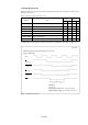
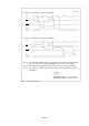
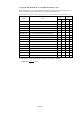
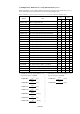

Table Of Contents
- Preface
- Contents
- 1. Precautions for Safety
- 2. Preparation
- 3. Setting Up
- 4. Usage
- 5. Specifications
- 6. Troubleshooting
- 6.1 Flowchart to Remedy the Troubles
- 6.2 When the Emulator Debugger Does Not Start Up Properly
- 6.3 Operation Differs from That of PROM Version MCUs
- (1) Does Not Operate with Operating Frequencies (3.6 V to 5.5 V) Properly
- (2) Does Not Operate with Operating Frequencies (2.7 V to 3.6 V) Properly
- (3) Cannot Reset from Target System
- (4) Data Values of ROM Area at Power-on Are Different
- (5) HOLD* control
- (6) A-D Conversion Values are Different from Expected Values
- (7) Outputs of ALE, Address and Others are Different from Those of Actual MCUs
- 7. Maintenance and Guarantee
( 60 / 78 )
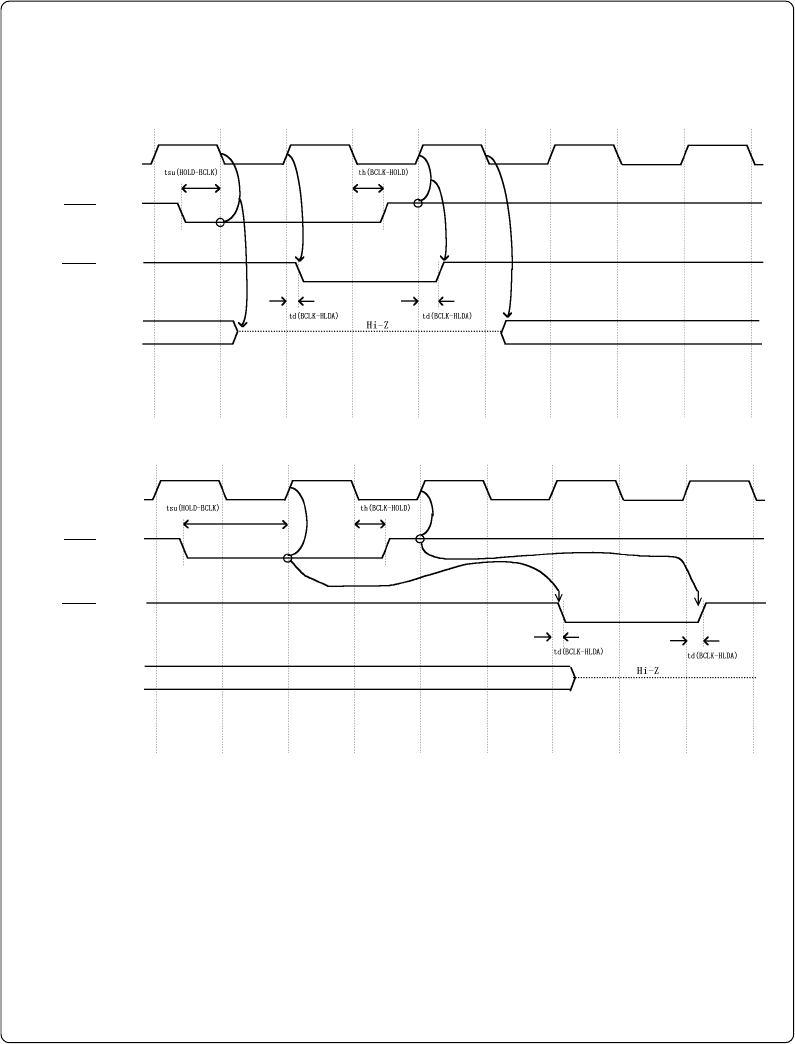
Figure 5.10 Timing requirements
VCC = 3 V
Memory expansion mode and microprocessor mode
Common to "with wait" and "no-wait" (actual MCU)
Common to "with wait" and "no-wait" (this product)
Note 1. P0
0 to P52 will be high-impedance status regardless of the input level of BYTE pin and
ports P40 to P43 function selection bit (PM06) of the processor mode register 0.
Note 2. This product will be high-impedance delaying by 2.5 cycles than an actual MCU.
Note 3. The setup time of HOLD is defined by the startup of BSLK, differently from that of
actual MCUs.
Conditions:
• V
CC =3 V
• Input timing voltage: VIL = 0.6 V, VIH = 2.4 V
• Output timing voltage: VOL = 1.5 V, VOH = 1.5 V
BCLK
BCLK
P0, P1, P2,
P3, P4,
P50 to P52
HOLD input
HOLD input
P0, P1, P2,
P3, P4,
P50 to P52
HLDA output
HLDA output