
Emulation Pod User's Manual
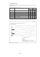
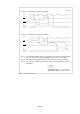
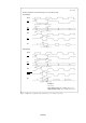
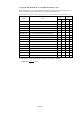
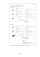

Table Of Contents
- Preface
- Contents
- 1. Precautions for Safety
- 2. Preparation
- 3. Setting Up
- 4. Usage
- 5. Specifications
- 6. Troubleshooting
- 6.1 Flowchart to Remedy the Troubles
- 6.2 When the Emulator Debugger Does Not Start Up Properly
- 6.3 Operation Differs from That of PROM Version MCUs
- (1) Does Not Operate with Operating Frequencies (3.6 V to 5.5 V) Properly
- (2) Does Not Operate with Operating Frequencies (2.7 V to 3.6 V) Properly
- (3) Cannot Reset from Target System
- (4) Data Values of ROM Area at Power-on Are Different
- (5) HOLD* control
- (6) A-D Conversion Values are Different from Expected Values
- (7) Outputs of ALE, Address and Others are Different from Those of Actual MCUs
- 7. Maintenance and Guarantee
( 59 / 78 )
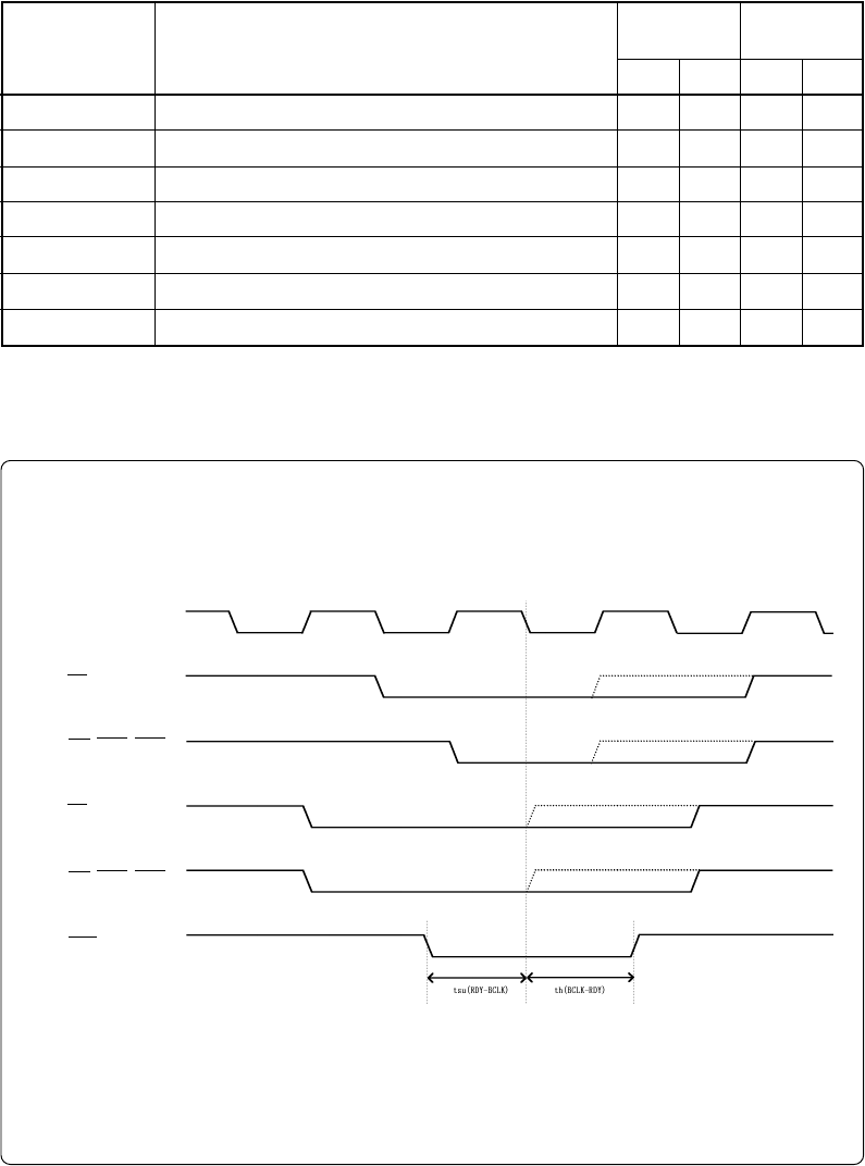
(4) Timing Requirements
Table 5.9, Figures 5.9 and 5.10 show timing requirements in the memory expansion mode and the
microprocessor mode.
Table 5.9 Timing requirements (VCC = 3 V)
*1 Minimum 7 ns (The definition is different from that of actual MCUs. For details, see Figure 5.10.)
Figure 5.9 Timing requirements
VCC = 3 V
Memory expansion mode and microprocessor mode
(only with wait)
BCLK
RD
(separate bus)
RD
(multiplex bus)
RDY input
WR, WRL, WRH
(separate bus)
WR, WRL, WRH
(multiplex bus)
Conditions:
• V
CC = 3 V
• Input timing voltage: VIL = 0.6 V, VIH = 2.4 V
• Output timing voltage: VOL = 1.5 V, VOH = 1.5 V
Tsu (DB-RD)
Tsu (RDY-BCLK)
Tsu (HOLD-BCLK)
Th (RD-DB)
Th (BCLK-RDY)
Th (BCLK-HOLD)
Td (BCLK-HDLA)
Data input setup time
RDY* input setup time
HOLD* input setup time
Data input hold time
RDY* input hold time
HOLD* input hold time
HLDA* output delay time
Min.
80
60
80
0
0
0
Max.
100
Min.
80
(*1)
Max.
Actual MCU
[ns]
This product
[ns]
Symbol
Item
See left
See left
See left
See left
See left