
Emulation Pod User's Manual
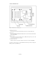
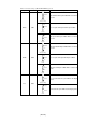
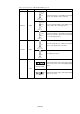
Table Of Contents
- Preface
- Contents
- 1. Precautions for Safety
- 2. Preparation
- 3. Setting Up
- 4. Usage
- 5. Specifications
- 6. Troubleshooting
- 6.1 Flowchart to Remedy the Troubles
- 6.2 When the Emulator Debugger Does Not Start Up Properly
- 6.3 Operation Differs from That of PROM Version MCUs
- (1) Does Not Operate with Operating Frequencies (3.6 V to 5.5 V) Properly
- (2) Does Not Operate with Operating Frequencies (2.7 V to 3.6 V) Properly
- (3) Cannot Reset from Target System
- (4) Data Values of ROM Area at Power-on Are Different
- (5) HOLD* control
- (6) A-D Conversion Values are Different from Expected Values
- (7) Outputs of ALE, Address and Others are Different from Those of Actual MCUs
- 7. Maintenance and Guarantee
( 26 / 78 )
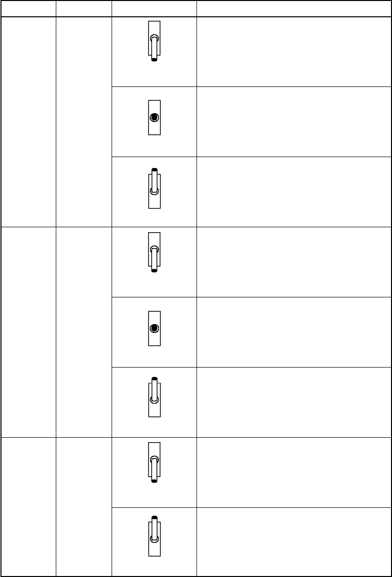
Table 3.1 Switch settings of M30620T2-RPD-E (part 1)
Signal Switch Setting Description
CNV
SS SW1
SW2BYTE
X
OUT SW3
Pulls down the CNV
SS pin of MCU with a resistance
at 33 kΩ.
Does not pull down/up the CNV
SS pin of MCU.
Pulls up the CNVSS pin of MCU with a resistance
at 33 kΩ.
Does not pull down/up the BYTE pin of MCU.
Pulls up the BYTE pin of MCU with a resistance at
33 kΩ.
Does not connect the X
OUT pin of MCU to the target
system.
Pulls down the BYTE pin of MCU with a resistance
at 33 kΩ.
Connects the X
OUT pin of MCU to the target system.
L
OPEN
H
SW1
CNVSS
(Factory-setting)
L
OPEN
H
SW1
CNVSS
L
OPEN
H
SW1
CNVSS
16
OPEN
8
SW2
BYTE
(Factory-setting)
16
OPEN
8
SW2
BYTE
16
OPEN
8
SW2
BYTE
OPEN
XOUT
SW3
XOUT
(Factory-setting)
OPEN
XOUT
SW3
XOUT