
Datasheet


Rev. 3.00 Mar. 15, 2006 Page 518 of 526
REJ09B0060-0300
Item Page Revision (See Manual for Details)
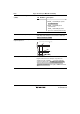
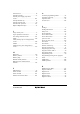
Figure 14.44 Example of Output
Disable Timing of Timer Z by
Writing to TOER
276 Amended
T
1
T
2
TOER
Address bus
TOER address
Timer Z
output pin
Timer Z output
I/O port
I/O port
Timer output
φ
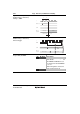
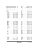
Figure 14.45 Example of Output
Disable Timing of Timer Z by
External Trigger
277 Amended
WKP4
TOER
Timer Z
output pin
Timer Z output I/O port
N H'FF
φ
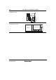
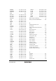
Amended
Bit Bit Name Description
4 TCSRWE Timer Control/Status Register WD
Write Enable
The WDON and WRST bits can
be written when the TCSRWE bit
is set to 1.
When writing data to this bit, the
value for bit 5 must be 0.
15.2.1 Timer Control/Status
Register WD (TCSRWD
290