
Datasheet


Appendix
Rev. 3.00 Mar. 15, 2006 Page 482 of 526
REJ09B0060-0300
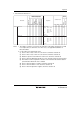
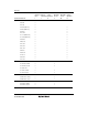
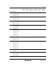
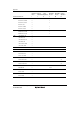
Table A.3 Number of Cycles in Each Instruction
Execution Status
Access Location
(Instruction Cycle) On-Chip Memory On-Chip Peripheral Module
Instruction fetch S
I
2 —
Branch address read S
J
Stack operation S
K
Byte data access S
L
2 or 3*
Word data access S
M
—
Internal operation S
N
1
Note: * Depends on which on-chip peripheral module is accessed. See section 22.1, Register
Addresses (Address Order).