
Datasheet


Section 23 Electrical Characteristics
Rev. 3.00 Mar. 15, 2006 Page 460 of 526
REJ09B0060-0300
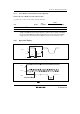
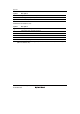
V
IH
V
IL
t
IL
NMI,
IRQ0 to IRQ3,
WKP0 to WKP5,
ADTRG,
FTIOA to FTIOD,
FTIOA0 to FTIOD0,
FTIOA1 to FTIOD1,
TMCIV, TMRIV,
TRGV, FTCI, TMIB1
t
IH
Figure 23.3 Input Timing
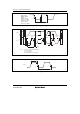
SCL
V
IH
V
IL
t
STAH
t
BUF
P* S*
t
Sf
t
SCL
t
SDAH
t
SCLH
t
SCLL
SDA
Sr*
t
STAS
t
SP
t
STOS
t
SDAS
P*
Note: * S, P, and Sr represent the following:
S: Start condition
P: Stop condition
Sr: Retransmission start condition
Figure 23.4 I
2
C Bus Interface Input/Output Timing
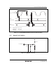
t
Scyc
t
SCKW
SCK3
Figure 23.5 SCK3 Input Clock Timing