
Datasheet


Section 23 Electrical Characteristics
Rev. 3.00 Mar. 15, 2006 Page 442 of 526
REJ09B0060-0300
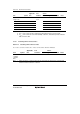
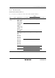
23.2.8 Power-On Reset Circuit Characteristics (Optional)
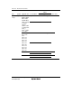
Table 23.10 Power-On Reset Circuit Characteristics
V
SS
= 0.0 V, T
a
= –20 to +75°C, unless otherwise indicated.
Values
Item Symbol
Test
Condition
Min. Typ. Max. Unit
Pull-up resistance of RES pin R
RES
100 150 kΩ
Power-on reset start voltage* V
por
100 mV
Note: * The power-supply voltage (Vcc) must fall below Vpor = 100 mV and then rise after
charge of the RES pin is removed completely. In order to remove charge of the RES
pin, it is recommended that the diode be placed in the Vcc side. If the power-supply
voltage (Vcc) rises from the point over 100 mV, a power-on reset may not occur.
23.3 Electrical Characteristics (Masked ROM Version)
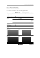
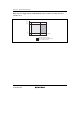
23.3.1 Power Supply Voltage and Operating Ranges
Power Supply Voltage and Oscillation Frequency Range
10.0
2.0
20.0
2.7 4.0 5.5 V
CC
(V)
φ
OSC
(MHz)
32.768
2.7 4.0 5.5 V
CC
(V)
φ
W
(kHz)
• AV
CC
= 2.7 to 5.5 V
• Active mode
• Sleep mode
• AV
CC
= 2.7 to 5.5 V
• All operating modes