
Datasheet

Section 23 Electrical Characteristics
Rev. 3.00 Mar. 15, 2006 Page 434 of 526
REJ09B0060-0300
Applicable
Values
Reference
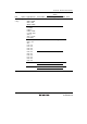
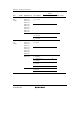
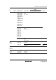
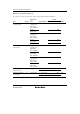
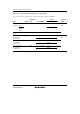
Item Symbol Pins Test Condition Min. Typ. Max. Unit Figure
RES pin low
width
t
REL
RES At power-on and in
modes other than
those below
t
rc
ms Figure
23.2
In active mode and
sleep mode
operation
200 ns
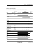
Input pin high
width
t
IH
NMI, TMBI1,
IRQ0 to
IRQ3,
WKP0 to
WKP5,
TMCIV,
TMRIV,
TRGV,
ADTRG,
FTIOA0 to
FTIOD0,
FTIOA1 to
FTIOD1,
FTIOA to
FTIOD, FTCI
2 t
cyc
t
subcyc
Figure
23.3
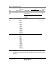
Input pin low
width
t
IL
NMI, TMBI1,
IRQ0 to
IRQ3,
WKP0 to
WKP5,
TMCIV,
TMRIV,
TRGV,
ADTRG,
FTIOA0 to
FTIOD0,
FTIOA1 to
FTIOD1,
FTIOA to
FTIOD, FTCI
2 t
cyc
t
subcyc
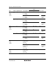
Notes: 1. When an external clock is input, the minimum system clock oscillation frequency is
1.0 MHz.
2. Determined by the MA2, MA1, MA0, SA1, and SA0 bits in the system control register 2
(SYSCR2).