
Datasheet


Section 22 List of Registers
Rev. 3.00 Mar. 15, 2006 Page 404 of 526
REJ09B0060-0300
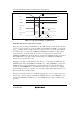
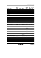
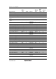
22.1 Register Addresses (Address Order)
The data-bus width column indicates the number of bits. The access-state column shows the
number of states of the specified basic clock that is required for access to the register.
Note: Access to undefined or reserved addresses is prohibited. Correct operation of the access
itself or later operations is not guaranteed when such a register is accessed.
Register Name
Abbre-
viation
Bit No.
Address
Module
Name
Data
Bus
Width
Access
State
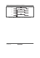
— — — H'FFF000 to
H'FFF5FF
— — —
Serial mode register_3 SMR_3 8 H'FFF600 SCI3_3 8 3
Bit rate register_3 BRR_3 8 H'FFF601 SCI3_3 8 3
Serial control register 3_3 SCR3_3 8 H'FFF602 SCI3_3 8 3
Transmit data register_3 TDR_3 8 H'FFF603 SCI3_3 8 3
Serial status register_3 SSR_3 8 H'FFF604 SCI3_3 8 3
Receive data register_3 RDR_3 8 H'FFF605 SCI3_3 8 3
— — — H'FFF606,
H'FFF607
— — —
Serial mode control register SMCR_3 8 H'FFF608 SCI3_3 8 3
— — — H'FFF609 to
H'FFF6FF
— — —
Timer control register_0 TCR_0 8 H'FFF700 Timer Z0 8 2
Timer I/O control register A_0 TIORA_0 8 H'FFF701 Timer Z0 8 2
Timer I/O control register C_0 TIORC_0 8 H'FFF702 Timer Z0 8 2
Timer status register_0 TSR_0 8 H'FFF703 Timer Z0 8 2
Timer interrupt enable register_0 TIER_0 8 H'FFF704 Timer Z0 8 2
PWM mode output level control
register_0
POCR_0 8 H'FFF705 Timer Z0 8 2
Timer counter_0 TCNT_0 16 H'FFF706 Timer Z0 16 2
General register A_0 GRA_0 16 H'FFF708 Timer Z0 16 2
General register B_0 GRB_0 16 H'FFF70A Timer Z0 16 2
General register C_0 GRC_0 16 H'FFF70C Timer Z0 16 2
General register D_0 GRD_0 16 H'FFF70E Timer Z0 16 2