
Datasheet


Section 20 Power-On Reset and Low-Voltage Detection Circuits (Optional)
Rev. 3.00 Mar. 15, 2006 Page 398 of 526
REJ09B0060-0300
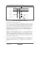
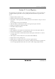
LVDRES
VCC
Vreset
VSS
V
LVDRmin
OVF
PSS-reset
signal
Internal reset
signal
131,072 cycles
PSS counter starts
Reset released
Figure 20.3 Operational Timing of LVDR Circuit
LVDI (Interrupt by Low Voltage Detect) Circuit:
Figure 20.4 shows the timing of LVDI functions. The LVDI enters the module-standby state after
a power-on reset is canceled. To operate the LVDI, set the LVDE bit in LVDCR to 1, wait for 50
µs (t
LVDON
) until the reference voltage and the low-voltage-detection power supply have stabilized
by a software timer, etc., then set the LVDDE and LVDUE bits in LVDCR to 1. After that, the
output settings of ports must be made. To cancel the low-voltage detection circuit, first the
LVDDE and LVDUE bits should all be cleared to 0 and then the LVDE bit should be cleared to 0.
The LVDE bit must not be cleared to 0 at the same timing as the LVDDE and LVDUE bits
because incorrect operation may occur.
When the power-supply voltage falls below Vint (D) (typ. = 3.7 V) voltage, the LVDI clears the
LVDINT signal to 0 and the LVDDF bit in LVDSR is set to 1. If the LVDDE bit is 1 at this time,
an IRQ0 interrupt request is simultaneously generated. In this case, the necessary data must be
saved in the external EEPROM, etc, and a transition must be made to standby mode or subsleep
mode. Until this processing is completed, the power supply voltage must be higher than the lower
limit of the guaranteed operating voltage.
When the power-supply voltage does not fall below Vreset1 (typ. = 2.3 V) voltage but rises above
Vint (U) (typ. = 4.0 V) voltage, the LVDI sets the LVDINT signal to 1. If the LVDUE bit is 1 at
this time, the LVDUF bit in LVDSR is set to 1 and an IRQ0 interrupt request is simultaneously
generated.