
Datasheet


Section 1 Overview
Rev. 3.00 Mar. 15, 2006 Page 5 of 526
REJ09B0060-0300
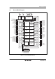
1.4 Pin Functions
Table 1.1 Pin Functions
Pin No.
Type Symbol FP-80A I/O Functions
Power
supply pins
Vcc 12 Input Power supply pin. Connect this pin to the
system power supply.
Vss 9, 50 Input Ground pin. Ensure to connect all pins to the
system power supply (0 V).
AVcc 3 Input Analog power supply pin for the A/D converter.
When the A/D converter is not used, connect
this pin to the system power supply.
AVss 74 Input Analog ground pin for the A/D converter.
Connect this pin to the system power supply
(0 V).
VCL 6 Input Internal step-down power supply pin. Connect a
capacitor of around 0.1 µF between this pin and
the Vss pin for stabilization.
Clock pins OSC1 11 Input
OSC2 10 Output
These pins connect with crystal or ceramic
resonator for the system clock, or can be used
to input an external clock.
See section 5, Clock Pulse Generators, for a
typical connection.
X1 5 Input
X2 4 Output
These pins connect with a 32.768 kHz crystal
resonator for the subclock. See section 5, Clock
Pulse Generators, for a typical connection.
System
control
RES 7 Input Reset pin. The pull-up resistor (typ.150 kΩ) is
incorporated. When driven low, the chip is reset.
TEST 8 Input Test pin. Connect this pin to Vss.
NMI 13 Input Non-maskable interrupt request input pin.
Be sure to pull-up by a pull-up resistor.
External
interrupt
pins
IRQ0 to
IRQ3
25 to 28 Input External interrupt request input pins. Can select
the rising or falling edge.
WKP0 to
WKP5
36 to 31 Input External interrupt request input pins. Can select
the rising or falling edge.
RTC TMOW 56 Output This is an output pin for divided clocks.
Timer B1 TMIB1 26 Input External event input pin.