
Datasheet


Section 17 Serial Communication Interface 3 (SCI3)
Rev. 3.00 Mar. 15, 2006 Page 307 of 526
REJ09B0060-0300
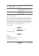
Bit Bit Name
Initial
Value R/W Description
1
0
CKE1
CKE0
0
0
R/W
R/W
Clock Enable 0 and 1
Selects the clock source.
• Asynchronous mode
00: On-chip baud rate generator
01: On-chip baud rate generator
Outputs a clock of the same frequency as the bit
rate from the SCK3 pin.
10: External clock
Inputs a clock with a frequency 16 times the bit rate
from the SCK3 pin.
11:Reserved
• Clocked synchronous mode
00: On-chip clock (SCK3 pin functions as clock output)
01:Reserved
10: External clock (SCK3 pin functions as clock input)
11:Reserved
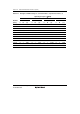
17.3.7 Serial Status Register (SSR)
SSR is a register containing status flags of the SCI3 and multiprocessor bits for transfer. 1 cannot
be written to flags TDRE, RDRF, OER, PER, and FER; they can only be cleared.
Bit Bit Name
Initial
Value R/W Description
7 TDRE 1 R/W Transmit Data Register Empty
Indicates whether TDR contains transmit data.
[Setting conditions]
• When the TE bit in SCR3 is 0
• When data is transferred from TDR to TSR
[Clearing conditions]
• When 0 is written to TDRE after reading TDRE = 1
• When the transmit data is written to TDR