
Datasheet


Section 17 Serial Communication Interface 3 (SCI3)
Rev. 3.00 Mar. 15, 2006 Page 303 of 526
REJ09B0060-0300
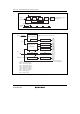
17.2 Input/Output Pins
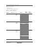
Table 17.2 shows the SCI3 pin configuration.
Table 17.2 Pin Configuration
Pin Name Abbreviation I/O Function
SCI3 clock SCK3 I/O SCI3 clock input/output
SCI3 receive data input RXD Input SCI3 receive data input
SCI3 transmit data output TXD Output SCI3 transmit data output
17.3 Register Descriptions
The SCI3 has the following registers for each channel.
• Receive Shift Register (RSR)
• Receive Data Register (RDR)
• Transmit Shift Register (TSR)
• Transmit Data Register (TDR)
• Serial Mode Register (SMR)
• Serial Control Register 3 (SCR3)
• Serial Status Register (SSR)
• Bit Rate Register (BRR)
• Serial mode control register 3 (SMCR3)
17.3.1 Receive Shift Register (RSR)
RSR is a shift register that is used to receive serial data input from the RxD pin and convert it into
parallel data. When one frame of data has been received, it is transferred to RDR automatically.
RSR cannot be directly accessed by the CPU.
17.3.2 Receive Data Register (RDR)
RDR is an 8-bit register that stores received data. When the SCI3 has received one frame of serial
data, it transfers the received serial data from RSR to RDR, where it is stored. After this, RSR is
receive-enabled. As RSR and RDR function as a double buffer in this way, continuous receive
operations are possible. After confirming that the RDRF bit in SSR is set to 1, read RDR only
once. RDR cannot be written to by the CPU. RDR is initialized to H'00.