
Datasheet


Section 17 Serial Communication Interface 3 (SCI3)
Rev. 3.00 Mar. 15, 2006 Page 299 of 526
REJ09B0060-0300
Section 17 Serial Communication Interface 3 (SCI3)
This LSI includes a serial communication interface 3 (SCI3), which has independent three
channels. The SCI3 can handle both asynchronous and clocked synchronous serial
communication. In asynchronous mode, serial data communication can be carried out using
standard asynchronous communication chips such as a Universal Asynchronous
Receiver/Transmitter (UART) or an Asynchronous Communication Interface Adapter (ACIA). A
function is also provided for serial communication between processors (multiprocessor
communication function).
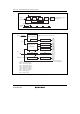
Table 17.1 shows the SCI3 channel configuration and figure 17.1 shows a block diagram of the
SCI3. Since basic pin functions are identical for each of the three channels (SCI3, SCI3_2, and
SCI3_3), separate explanations are not given in this section.
17.1 Features
• Choice of asynchronous or clocked synchronous serial communication mode
• Full-duplex communication capability
The transmitter and receiver are mutually independent, enabling transmission and reception to
be executed simultaneously.
Double-buffering is used in both the transmitter and the receiver, enabling continuous
transmission and continuous reception of serial data.
• On-chip baud rate generator allows any bit rate to be selected
• External clock or on-chip baud rate generator can be selected as a transfer clock source.
• Six interrupt sources
Transmit-end, transmit-data-empty, receive-data-full, overrun error, framing error, and parity
error.
• Noise canceller (only for SCI3_3)
Asynchronous mode
• Data length: 7 or 8 bits
• Stop bit length: 1 or 2 bits
• Parity: Even, odd, or none
• Receive error detection: Parity, overrun, and framing errors
• Break detection: Break can be detected by reading the RxD pin level directly in the case of a
framing error