
Datasheet

Section 14 Timer Z
Rev. 3.00 Mar. 15, 2006 Page 268 of 526
REJ09B0060-0300
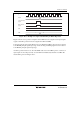
d. Buffer operation is used and other than TPSC2 = TPSC1 = TPSC0 = 0
Write a value which satisfies GRA_0 + 1 < GR < H'FFFF to the buffer register. A
waveform with a duty cycle of 0% can be output. However, a waveform with a duty
cycle of 100% cannot be output using the buffer operation. Also, the buffer operation
cannot be used to change duty cycles while a waveform with a duty cycle of 100% is
being output. For details on buffer operation, see section 14.4.8, Buffer Operation.
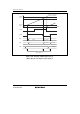
14.4.8 Buffer Operation
Buffer operation differs depending on whether GR has been designated for an input capture
register or an output compare register, or in reset synchronous PWM mode or complementary
PWM mode.
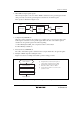
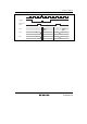
Table 14.8 shows the register combinations used in buffer operation.
Table 14.8 Register Combinations in Buffer Operation
General Register Buffer Register
GRA GRC
GRB GRD
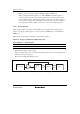
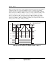
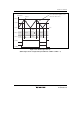
1. When GR is an output compare register
When a compare match occurs, the value in the buffer register of the corresponding channel is
transferred to the general register.
This operation is illustrated in figure 14.35.
Buffer register Comparator TCNT
General
register
Compare match signal
Figure 14.35 Compare Match Buffer Operation