
Datasheet

Section 14 Timer Z
Rev. 3.00 Mar. 15, 2006 Page 258 of 526
REJ09B0060-0300
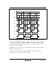
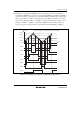
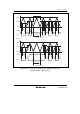
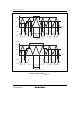
14.4.7 Complementary PWM Mode
Three PWM waveforms for non-overlapped normal and counter phases are output by combining
channels 0 and 1.
In complementary PWM mode, the FTIOB0 to FTIOD0 and FTIOA1 to FTIOD1 pins become
PWM-output pins automatically. TCNT_0 and TCNT_1 perform an increment or decrement
operation. Tables 14.6 and 14.7 show the output pins and register settings in complementary PWM
mode, respectively.
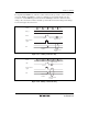
Figure 14.29 shows the example of complementary PWM mode setting procedure.
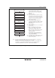
Table 14.6 Output Pins in Complementary PWM Mode
Channel Pin Name Input/Output Pin Function
0 FTIOC0 Output Toggle output in synchronous with PWM cycle
0 FTIOB0 Output PWM output 1
0 FTIOD0 Output PWM output 1 (counter-phase waveform non-
overlapped with PWM output 1)
1 FTIOA1 Output PWM output 2
1 FTIOC1 Output PWM output 2 (counter-phase waveform non-
overlapped with PWM output 2)
1 FTIOB1 Output PWM output 3
1 FTIOD1 Output PWM output 3 (counter-phase waveform non-
overlapped with PWM output 3)
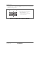
Table 14.7 Register Settings in Complementary PWM Mode
Register Description
TCNT_0 Initial setting of non-overlapped periods (non-overlapped periods are differences with
TCNT_1)
TCNT_1 Initial setting of H'0000
GRA_0 Sets (upper limit value – 1) of TCNT_0
GRB_0 Set a changing point of the PWM waveform output from pins FTIOB0 and FTIOD0.
GRA_1 Set a changing point of the PWM waveform output from pins FTIOA1 and FTIOC1.
GRB_1 Set a changing point of the PWM waveform output from pins FTIOB1 and FTIOD1.