
Datasheet

Section 14 Timer Z
Rev. 3.00 Mar. 15, 2006 Page 257 of 526
REJ09B0060-0300
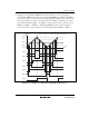
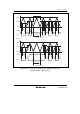
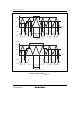
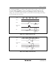
GRA_0
GRB_0
GRA_1
GRB_1
H'0000
FTIOA1
FTIOB1
FTIOB0
FTIOC1
FTIOD1
FTIOC0
FTIOD0
TCNT value
Counter cleared by GRA compare match
Time
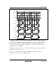
Figure 14.28 Example of Reset Synchronous PWM Mode Operation (OLS0 = OLS1 = 0)
In reset synchronous PWM mode, TCNT_0 and TCNT_1 perform increment and independent
operations, respectively. However, GRA_1 and GRB_1 are separated from TCNT_1. When a
compare match occurs between TCNT_0 and GRA_0, a counter is cleared and an increment
operation is restarted from H'0000.
The PWM pin outputs 0 or 1 whenever a compare match between GRB_0, GRA_1, GRB_1 and
TCNT_0 or counter clearing occur.
For details on operations when reset synchronous PWM mode and buffer operation are
simultaneously set, see section 14.4.8, Buffer Operation.