
Datasheet

Section 14 Timer Z
Rev. 3.00 Mar. 15, 2006 Page 249 of 526
REJ09B0060-0300
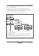
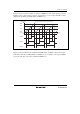
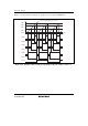
Figure 14.21 shows an example of the PWM mode setting procedure.
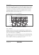
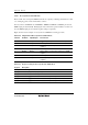
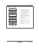
Table 14.3 Initial Output Level of FTIOB0 Pin
TOB0 POLB Initial Output Level
0 0 1
0 1 0
1 0 0
1 1 1
[1] Select the counter clock with bits TPSC2 to
TOSC0 in TCR. When an external clock is
selected, select the external clock edge with
bits CKEG1 and CKEG0 in TCR.
[2] Use bits CCLR1 and CCLR0 in TCR to select
the counter clearing source.
[3] Select the PWM mode with bits PWMB0 to
PWMD0 and PWMB1 to PWMD1 in TPMR.
[4] Set the initial output value with bits TOB0 to
TOD0 and TOB1 to TOD1 in TOCR.
[5] Set the output level with bits POLB to POLD in
POCR.
[6] Set the cycle in GRA, and set the duty in the
other GR.
[7] Enable or disable the timer output by TOER.
[8] Set the STR bit in TSTR to 1 and start the
counter operation.
[1]
[2]
[3]
[4]
[5]
[6]
[7]
PWM mode
Select counter clock
Select counter clearing source
Set PWM mode
Set initial output level
Select output level
Set GR
Enable waveform output
[8]
Start counter operation
<PWM mode>
Figure 14.21 Example of PWM Mode Setting Procedure