
Datasheet
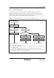

Section 14 Timer Z
Rev. 3.00 Mar. 15, 2006 Page 248 of 526
REJ09B0060-0300
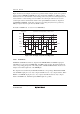
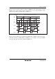
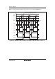
Figure 14.20 shows an example of synchronous operation. In this example, synchronous operation
has been selected, FTIOB0 and FTIOB1 have been designated for PWM mode, GRA_0 compare
match has been set as the channel 0 counter clearing source, and synchronous clearing has been set
for the channel 1 counter clearing source. In addition, the same input clock has been set as the
counter input clock for channel 0 and channel 1. Two-phase PWM waveforms are output from
pins FTIOB0 and FTIOB1. At this time, synchronous presetting and synchronous operation by
GRA_0 compare match are performed by TCNT counters.
For details on PWM mode, see section 14.4.5, PWM Mode.
GRA_0
Time
Synchronous clearing by GRA_0 compare match
TCNT values
GRA_1
GRB_0
GRB_1
H'0000
FTIOB0
FTIOB1
Figure 14.20 Example of Synchronous Operation
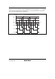
14.4.5 PWM Mode
In PWM mode, PWM waveforms are output from the FTIOB, FTIOC, and FTIOD output pins
with GRA as a cycle register and GRB, GRC, and GRD as duty registers. The initial output level
of the corresponding pin depends on the setting values of TOCR and POCR. Table 14.3 shows an
example of the initial output level of the FTIOB0 pin.
The output level is determined by the POLB to POLD bits corresponding to POCR. When POLB
is 0, the FTIOB output pin is set to 0 by compare match B and set to 1 by compare match A. When
POLB is 1, the FTIOB output pin is set to 1 by compare match B and cleared to 0 by compare
match A. In PWM mode, maximum 6-phase PWM outputs are possible.