
Datasheet


Section 13 Timer W
Rev. 3.00 Mar. 15, 2006 Page 201 of 526
REJ09B0060-0300
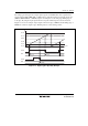
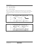
Figure 13.11 shows an example of buffer operation when the FTIOB pin is set to PWM mode and
GRD is set as the buffer register for GRB. TCNT is cleared by compare match A, and FTIOB
outputs 1 at compare match B and 0 at compare match A.
Due to the buffer operation, the FTIOB output level changes and the value of buffer register GRD
is transferred to GRB whenever compare match B occurs. This procedure is repeated every time
compare match B occurs.
TCNT value
GRA
H'0000
GRD
Time
GRB
H'0200 H'0520
FTIOB
H'0200
H'0450
H'0520
H'0450
GRB
H'0450 H'0520
H'0200
Figure 13.11 Buffer Operation Example (Output Compare)