
Datasheet

Section 13 Timer W
Rev. 3.00 Mar. 15, 2006 Page 190 of 526
REJ09B0060-0300
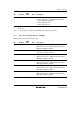
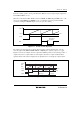
Bit Bit Name
Initial
Value R/W Description
5
4
IOB1
IOB0
0
0
R/W
R/W
I/O Control B1 and B0
When IOB2 = 0,
00: No output at compare match
01: 0 output to the FTIOB pin at GRB compare match
10: 1 output to the FTIOB pin at GRB compare match
11: Output toggles to the FTIOB pin at GRB compare
match
When IOB2 = 1,
00: Input capture at rising edge at the FTIOB pin
01: Input capture at falling edge at the FTIOB pin
1x: Input capture at rising edge and falling edge at the
FTIOB pin
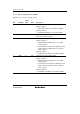
3 1 Reserved
This bit is always read as 1.
2 IOA2 0 R/W I/O Control A2
Selects the GRA function.
0: GRA functions as an output compare register
1: GRA functions as an input capture register
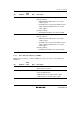
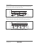
1
0
IOA1
IOA0
0
0
R/W
R/W
I/O Control A1 and A0
When IOA2 = 0,
00: No output at compare match
01: 0 output to the FTIOA pin at GRA compare match
10: 1 output to the FTIOA pin at GRA compare match
11: Output toggles to the FTIOA pin at GRA compare
match
When IOA2 = 1,
00: Input capture at rising edge of the FTIOA pin
01: Input capture at falling edge of the FTIOA pin
1x: Input capture at rising edge and falling edge of the
FTIOA pin
[Legend] X: Don't care.