
Datasheet

Section 13 Timer W
Rev. 3.00 Mar. 15, 2006 Page 187 of 526
REJ09B0060-0300
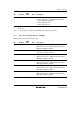
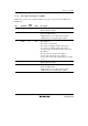
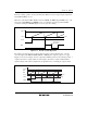
Bit Bit Name
Initial
Value R/W Description
0 TOA 0 R/W Timer Output Level Setting A
Sets the output value of the FTIOA pin until the first
compare match A is generated.
0: Initial output value is 0*
1: Initial output value is 1*
[Legend]
x: Don't care.
Note: * The change of the setting is immediately reflected in the output value.
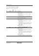
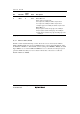
13.3.3 Timer Interrupt Enable Register W (TIERW)
TIERW controls the timer W interrupt request.
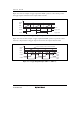
Bit Bit Name
Initial
Value R/W Description
7 OVIE 0 R/W Timer Overflow Interrupt Enable
When this bit is set to 1, FOVI interrupt requested by
OVF flag in TSRW is enabled.
6 to 4
All 1 Reserved
These bits are always read as 1.
3 IMIED 0 R/W Input Capture/Compare Match Interrupt Enable D
When this bit is set to 1, IMID interrupt requested by
IMFD flag in TSRW is enabled.
2 IMIEC 0 R/W Input Capture/Compare Match Interrupt Enable C
When this bit is set to 1, IMIC interrupt requested by
IMFC flag in TSRW is enabled.
1 IMIEB 0 R/W Input Capture/Compare Match Interrupt Enable B
When this bit is set to 1, IMIB interrupt requested by
IMFB flag in TSRW is enabled.
0 IMIEA 0 R/W Input Capture/Compare Match Interrupt Enable A
When this bit is set to 1, IMIA interrupt requested by
IMFA flag in TSRW is enabled.