
Datasheet


Section 13 Timer W
Rev. 3.00 Mar. 15, 2006 Page 185 of 526
REJ09B0060-0300
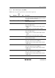
13.3.1 Timer Mode Register W (TMRW)
TMRW selects the general register functions and the timer output mode.
Bit Bit Name
Initial
Value R/W Description
7 CTS 0 R/W Counter Start
The counter operation is halted when this bit is 0; while
it can be performed when this bit is 1.
6 1 Reserved
This bit is always read as 1.
5 BUFEB 0 R/W Buffer Operation B
Selects the GRD function.
0: GRD operates as an input capture/output compare
register
1: GRD operates as the buffer register for GRB
4 BUFEA 0 R/W Buffer Operation A
Selects the GRC function.
0: GRC operates as an input capture/output compare
register
1: GRC operates as the buffer register for GRA
3 1 Reserved
This bit is always read as 1.
2 PWMD 0 R/W PWM Mode D
Selects the output mode of the FTIOD pin.
0: FTIOD operates normally (output compare output)
1: PWM output
1 PWMC 0 R/W PWM Mode C
Selects the output mode of the FTIOC pin.
0: FTIOC operates normally (output compare output)
1: PWM output
0 PWMB 0 R/W PWM Mode B
Selects the output mode of the FTIOB pin.
0: FTIOB operates normally (output compare output)
1: PWM output