
Datasheet


Section 12 Timer V
Rev. 3.00 Mar. 15, 2006 Page 179 of 526
REJ09B0060-0300
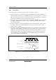
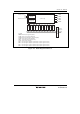
φ
Address
TCORA address
Internal write signal
TCNTV
TCORA
N
N
N+1
M
TCORA write data
Inhibited
T
1
T
2
T
3
TCORA write cycle by CPU
Compare match signal
Figure 12.12 Contention between TCORA Write and Compare Match
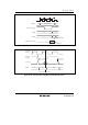
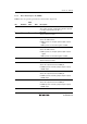
Clock before
switching
Clock after
switching
Count clock
TCNTV N N+1 N+2
Write to CKS1 and CKS0
Figure 12.13 Internal Clock Switching and TCNTV Operation