
Datasheet


Section 7 ROM
Rev. 3.00 Mar. 15, 2006 Page 106 of 526
REJ09B0060-0300
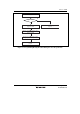
The FLMCR1, FLMCR2, and EBR1 settings are retained, however program mode or erase mode
is aborted at the point at which the error occurred. Program mode or erase mode cannot be re-
entered by re-setting the P or E bit. However, PV and EV bit settings are retained, and a transition
can be made to verify mode. Error protection can be cleared only by a power-on reset.
7.6 Programmer Mode
In programmer mode, a PROM programmer can be used to perform programming/erasing via a
socket adapter, just as a discrete flash memory. Use a PROM programmer that supports the MCU
device type with the on-chip Renesas Technology 128-kbyte flash memory.
7.7 Power-Down States for Flash Memory
In user mode, the flash memory will operate in either of the following states:
• Normal operating mode
The flash memory can be read and written to at high speed.
• Power-down operating mode
The power supply circuit of flash memory can be partly halted. As a result, flash memory can
be read with low power consumption.
• Standby mode
All flash memory circuits are halted.
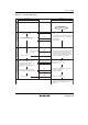
Table 7.7 shows the correspondence between the operating modes of this LSI and the flash
memory. In subactive mode, the flash memory can be set to operate in power-down mode with the
PDWND bit in FLPWCR. When the flash memory returns to its normal operating state from
power-down mode or standby mode, a period to stabilize operation of the power supply circuits
that were stopped is needed. When the flash memory returns to its normal operating state, bits
STS2 to STS0 in SYSCR1 must be set to provide a wait time of at least 20 µs, even when the
external clock is being used.