
Datasheet


Section 7 ROM
Rev. 3.00 Mar. 15, 2006 Page 103 of 526
REJ09B0060-0300
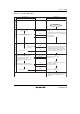
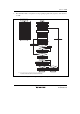
7.4.2 Erase/Erase-Verify
When erasing flash memory, the erase/erase-verify flowchart shown in figure 7.4 should be
followed.
1. Prewriting (setting erase block data to all 0s) is not necessary.
2. Erasing is performed in block units. Make only a single-bit specification in the erase block
register (EBR1). To erase multiple blocks, each block must be erased in turn.
3. The time during which the E bit is set to 1 is the flash memory erase time.
4. The watchdog timer (WDT) is set to prevent overerasing due to program runaway, etc. An
overflow cycle of approximately 19.8 ms is allowed.
5. For a dummy write to a verify address, write 1-byte data H'FF to an address whose lower two
bits are B'00. Verify data can be read in longwords from the address to which a dummy write
was performed.
6. If the read data is not erased successfully, set erase mode again, and repeat the erase/erase-
verify sequence as before. The maximum number of repetitions of the erase/erase-verify
sequence is 100.
7.4.3 Interrupt Handling when Programming/Erasing Flash Memory
All interrupts, including the NMI interrupt, are disabled while flash memory is being programmed
or erased, or while the boot program is executing, for the following three reasons:
1. Interrupt during programming/erasing may cause a violation of the programming or erasing
algorithm, with the result that normal operation cannot be assured.
2. If interrupt exception handling starts before the vector address is written or during
programming/erasing, a correct vector cannot be fetched and the CPU malfunctions.
3. If an interrupt occurs during boot program execution, normal boot mode sequence cannot be
carried out.