
Datasheet


Section 7 ROM
Rev. 3.00 Mar. 15, 2006 Page 100 of 526
REJ09B0060-0300
7.4 Flash Memory Programming/Erasing
A software method using the CPU is employed to program and erase flash memory in the on-
board programming modes. Depending on the FLMCR1 setting, the flash memory operates in one
of the following four modes: Program mode, program-verify mode, erase mode, and erase-verify
mode. The programming control program in boot mode and the user program/erase control
program in user program mode use these operating modes in combination to perform
programming/erasing. Flash memory programming and erasing should be performed in
accordance with the descriptions in section 7.4.1, Program/Program-Verify and section 7.4.2,
Erase/Erase-Verify, respectively.
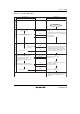
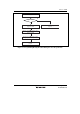
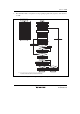
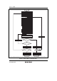
7.4.1 Program/Program-Verify
When writing data or programs to the flash memory, the program/program-verify flowchart shown
in figure 7.3 should be followed. Performing programming operations according to this flowchart
will enable data or programs to be written to the flash memory without subjecting the chip to
voltage stress or sacrificing program data reliability.
1. Programming must be done to an empty address. Do not reprogram an address to which
programming has already been performed.
2. Programming should be carried out 128 bytes at a time. A 128-byte data transfer must be
performed even if writing fewer than 128 bytes. In this case, H'FF data must be written to the
extra addresses.
3. Prepare the following data storage areas in RAM: A 128-byte programming data area, a 128-
byte reprogramming data area, and a 128-byte additional-programming data area. Perform
reprogramming data computation according to table 7.4, and additional programming data
computation according to table 7.5.
4. Consecutively transfer 128 bytes of data in byte units from the reprogramming data area or
additional-programming data area to the flash memory. The program address and 128-byte
data are latched in the flash memory. The lower 8 bits of the start address in the flash memory
destination area must be H'00 or H'80.
5. The time during which the P bit is set to 1 is the programming time. Table 7.6 shows the
allowable programming times.
6. The watchdog timer (WDT) is set to prevent overprogramming due to program runaway, etc.
An overflow cycle of approximately 6.6 ms is allowed.
7. For a dummy write to a verify address, write 1-byte data H'FF to an address whose lower 2
bits are B'00. Verify data can be read in words or in longwords from the address to which a
dummy write was performed.