
Datasheet


Section 7 ROM
Rev. 3.00 Mar. 15, 2006 Page 91 of 526
REJ09B0060-0300
7.2 Register Descriptions
The flash memory has the following registers.
• Flash memory control register 1 (FLMCR1)
• Flash memory control register 2 (FLMCR2)
• Erase block register 1 (EBR1)
• Flash memory power control register (FLPWCR)
• Flash memory enable register (FENR)
7.2.1 Flash Memory Control Register 1 (FLMCR1)
FLMCR1 is a register that makes the flash memory change to program mode, program-verify
mode, erase mode, or erase-verify mode. For details on register setting, refer to section 7.4, Flash
Memory Programming/Erasing.
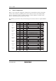
Bit Bit Name
Initial
Value R/W Description
7 — 0 — Reserved
This bit is always read as 0.
6 SWE 0 R/W Software Write Enable
When this bit is set to 1, flash memory
programming/erasing is enabled. When this bit is
cleared to 0, other FLMCR1 register bits and all EBR1
bits cannot be set.
5 ESU 0 R/W Erase Setup
When this bit is set to 1, the flash memory changes to
the erase setup state. When it is cleared to 0, the
erase setup state is cancelled. Set this bit to 1 before
setting the E bit to 1 in FLMCR1.
4 PSU 0 R/W Program Setup
When this bit is set to 1, the flash memory changes to
the program setup state. When it is cleared to 0, the
program setup state is cancelled. Set this bit to 1
before setting the P bit in FLMCR1.
3 EV 0 R/W Erase-Verify
When this bit is set to 1, the flash memory changes to
erase-verify mode. When it is cleared to 0, erase-verify
mode is cancelled.