
Datasheet


Section 12 Programmable Pulse Generator (PPG)
(This function is not available in the H8S/2695)
Page 644 of 1434 R01UH0166EJ0600 Rev. 6.00
Mar 02, 2011
H8S/2633 Group, H8S/2633 F-ZTAT
TM
,
H8S/2633R F-ZTAT
TM
, H8S/2695
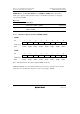
Address H'FE2D
Bit : 7 6 5 4 3 2 1 0
NDR7 NDR6 NDR5 NDR4 NDR3 NDR2 NDR1 NDR0
Initial value : 0 0 0 0 0 0 0 0
R/W : R/W R/W R/W R/W R/W R/W R/W R/W
Address H'FE2F
Bit : 7 6 5 4 3 2 1 0
— — — — — — — —
Initial value : 1 1 1 1 1 1 1 1
R/W : — — — — — — — —
Different Triggers for Pulse Output Groups: If pulse output groups 2 and 3 are triggered by
different compare match events, the address of the upper 4 bits in NDRH (group 3) is H'FE2C and
the address of the lower 4 bits (group 2) is H'FE2E. Bits 3 to 0 of address H'FE2C and bits 7 to 4
of address H'FE2E are reserved bits that cannot be modified and are always read as 1.
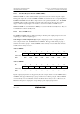
Address H'FE2C
Bit : 7 6 5 4 3 2 1 0
NDR15 NDR14 NDR13 NDR12 — — — —
Initial value : 0 0 0 0 1 1 1 1
R/W : R/W R/W R/W R/W — — — —
Address H'FE2E
Bit : 7 6 5 4 3 2 1 0
— — — — NDR11 NDR10 NDR9 NDR8
Initial value : 1 1 1 1 0 0 0 0
R/W : — — — — R/W R/W R/W R/W
If pulse output groups 0 and 1 are triggered by different compare match event, the address of the
upper 4 bits in NDRL (group 1) is H'FE2D and the address of the lower 4 bits (group 0) is
H'FE2F. Bits 3 to 0 of address H'FE2D and bits 7 to 4 of address H'FE2F are reserved bits that
cannot be modified and are always read as 1. However, the H8S/2633 Group has no output pins
corresponding to pulse output groups 0 and 1.