
Datasheet


Section 11 16-Bit Timer Pulse Unit (TPU)
Page 598 of 1434 R01UH0166EJ0600 Rev. 6.00
Mar 02, 2011
H8S/2633 Group, H8S/2633 F-ZTAT
TM
,
H8S/2633R F-ZTAT
TM
, H8S/2695
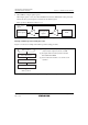
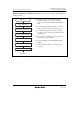
Examples of Buffer Operation
• When TGR is an output compare register
Figure 11.19 shows an operation example in which PWM mode 1 has been designated for
channel 0, and buffer operation has been designated for TGRA and TGRC. The settings used
in this example are TCNT clearing by compare match B, 1 output at compare match A, and 0
output at compare match B.
As buffer operation has been set, when compare match A occurs the output changes and the
value in buffer register TGRC is simultaneously transferred to timer general register TGRA.
This operation is repeated each time compare match A occurs.
For details of PWM modes, see section 11.4.6, PWM Modes.
TCNT value
TGR0B
H'0000
TGR0C
Time
TGR0A
H'0200 H'0520
TIOCA
H'0200
H'0450
H'0520
H'0450
TGR0A
H'0450H'0200
Transfer
Figure 11.19 Example of Buffer Operation (1)