
Datasheet


Section 10B I/O Ports
(H8S/2695)
R01UH0166EJ0600 Rev. 6.00 Page 483 of 1434
Mar 02, 2011
H8S/2633 Group, H8S/2633 F-ZTAT
TM
,
H8S/2633R F-ZTAT
TM
, H8S/2695
Pin Selection Method and Pin Functions
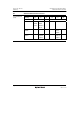
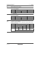
P34/RxD1 Switches as follows according to combinations of ICCR0 ICE bit of IIC0, SCR RE bit
of SCI1, and the P34DDR bit.
RE 0 1
P34DDR 0 1 —
Pin function P34 input pin P34 output pin
*
RxD1 input pin
Note: * Output type is NMOS push-pull. When P34ODR = 1, it becomes NMOS
open drain tray.
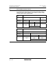
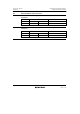
P33/TxD1 Switches as follows according to combinations of ICCR1 ICE bit of IIC1, SCR TE bit
of SCI1 and the P33DDR bit.
TE 0 1
P33DDR 0 1 —
Pin function P33 input pin P33 output pin
*
TxD1 output pin
*
Note: * When P33ODR = 1, it becomes NMOS open drain output.
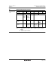
P32/SCK0/
IRQ4
Switches as follows according to combinations of SMR C/A bit of SCI0, SCR CKE0
and CKE1 bits, and the P32DDR bit.
If using as an SDA1 input pin, always set SMR C/A bit of SCI0 and SCR CKE0 and
CKE1 bits to 0 without fail.
CKE1 0 1
C/A 0 1 —
CKE0 0 1 — —
P32DDR 0 1 — — —
Pin function P32
input pin
P32
output pin
SCK0 output
pin
*
SCK0 output
pin
*
SCK0
input pin
IRQ4 input
Note: * When P32ODR = 1, it becomes NMOS open drain output.