
Datasheet


Section 22 ROM
R01UH0166EJ0600 Rev. 6.00 Page 961 of 1434
Mar 02, 2011
H8S/2633 Group, H8S/2633 F-ZTAT
TM
,
H8S/2633R F-ZTAT
TM
, H8S/2695
Bit 4—I
2
C Master Enable (IICE): Controls access to the I
2
C bus interface data registers and
control registers (ICCR, ICSR, ICDR/SARX, and ICMR/SAR). For details of the control, see
section 18.2.7, Serial Control Register X (SCRX).
Bit 3—Flash Memory Control Register Enable (FLSHE): Controls CPU access to the flash
memory control registers (FLMCR1, FLMCR2, EBR1, and EBR2). Setting the FLSHE bit to 1
enables read/write access to the flash memory control registers. If FLSHE is cleared to 0, the flash
memory control registers are deselected. In this case, the flash memory control register contents
are retained.
Bit 3
FLSHE Description
0 Flash control registers deselected in area H'FFFFA8 to H'FFFFAC (Initial value)
1 Flash control registers selected in area H'FFFFA8 to H'FFFFAC
Bits 2 to 0—Reserved: Should always be written with 0.
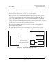
22.6 On-Board Programming Modes
When pins are set to on-board programming mode and a reset-start is executed, a transition is
made to the on-board programming state in which program/erase/verify operations can be
performed on the on-chip flash memory. There are two on-board programming modes: boot mode
and user program mode. The pin settings for transition to each of these modes are shown in table
22.9. For a diagram of the transitions to the various flash memory modes, see figure 22.11.
Table 22.9 Setting On-Board Programming Modes
Mode FWE MD2 MD1 MD0
Boot mode Expanded mode 1 0 1 0
Single-chip mode 0 1 1
User program mode Expanded mode 1 1 1 0
Single-chip mode 1 1 1