
Datasheet


Appendix A Instruction Set
Rev.7.00 Feb. 14, 2007 page 921 of 1108
REJ09B0089-0700
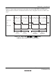
Figure A.1 shows timing waveforms for the address bus and the RD, HWR, and LWR signals
during execution of the above instruction with an 8-bit bus, using three-state access with no wait
states.
φ
A
ddress bus
RD
HWR, LWR
R:W 2nd
Fetching
2nd byte of
instruction at
jump address
Fetching
1st byte of
instruction at
jump address
Fetching
4th byte
of instruction
Fetching
3rd byte
of instruction
R:W EA
High
Internal
operation
Figure A.1 Address Bus, RD, HWR, and LWR Timing
(8-Bit Bus, Three-State Access, No Wait States)