
Datasheet


Rev.7.00 Feb. 14, 2007 page vii of xxxii
REJ09B0089-0700
Main Revisions for This Edition
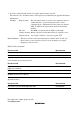
Item Page Revision (See Manual for Details)
1.3.1 Pin
Arrangement
Figure 1.6
HD64F2319CLP,
HD6432317SLP,
HD6432316SLP Pin
Arrangement (TLP-
113V: Top View)
13 Figure 1.6 amended
(Before) TLP-113V (Top View) → (After) (Top View)
2.6.3 Table of
Instructions Classified
by Function
Table 2.3
Instructions Classified
by Function
45 Table 2.3 amended
MOVFPE, MOVTPE (Before) Cannot be used in the H8S/2357
Series. → (After) Cannot be used in the H8S/2319 Group.
6.3.5 Chip Select
Signals
156 Description amended
... the data direction register (DDR) ,CS167 Enable(CS167E),
CS25 Enable, CSS17, CSS36, PF1CS5S, PF0CS4S for the
port corresponding to the particular CSn pin. ... the
corresponding control registers bits should be set when
outputting signals CS1 to CS7. ... the corresponding control
registers bits should be set when outputting signals CS0 to
CS7. ...
8.2.2 Register
Configuration
223, 224 Port 1 Data Direction Register (P1DDR)
Port 1 Data Register (P1DR)
Port 1 Register (PORT1)
Description amended
(Before) ... retains its prior state after in software standby mode.
→ (After) ... retains its prior state in software standby mode.
8.3.2 Register
Configuration
236, 237 Port 2 Data Direction Register (P2DDR)
Port 2 Data Register (P2DR)
Port 2 Register (PORT2)
Description amended
(Before) ... retains its prior state after in software standby mode.
→ (After) ... retains its prior state in software standby mode.