
Datasheet


Section 20 Electrical Characteristics
Rev.7.00 Feb. 14, 2007 page 853 of 1108
REJ09B0089-0700
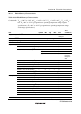
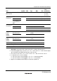
Item
Symbol
Min
Typ
Max
Unit
Test
Conditions
Input pull-up
MOS current
Ports A to E –I
p
10 — 300 μA V
CC
= 3.0 V
to 3.6 V,
V
in
= 0 V
RES — — 30 pF V
in
= 0 V
NMI — — 30 pF f = 1 MHz
Input
capacitance
All input pins
except RES and
NMI
C
in
— — 15 pF T
a
= 25°C
Normal operation — 25 (3.3 V) 50 mA
Sleep mode 17 (3.3 V) 40 mA
f = 25 MHz
— 20 90 μA T
a
≤ 50°C
Current
dissipation
*
2
Standby mode
*
3
I
CC
*
4
— — 120 μA 50°C < T
a
During A/D and
D/A conversion
— 1.0
(3.0 V)
2.0 mA Analog
power
supply
voltage
Idle
AI
CC
— 1.0 5.0 μA
During A/D and
D/A conversion
— 1.4
(3.0 V)
3.0 mA Reference
power
supply
voltage
Idle
AI
CC
— 0.2 5.0 μA
RAM standby voltage V
RAM
2.5 — — V
VCC start voltage
*
5
VCC
START
— — 0.4 V
VCC rising edge
*
5
SVCC — — 10 ms/V
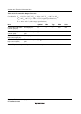
Notes: 1. If the A/D and D/A converters are not used, do not leave the AV
CC
, V
ref
, and AV
SS
pins open. Connect the AV
CC
and V
ref
pins to V
CC
, and the AV
SS
pin to V
SS
.
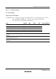
2. Current dissipation values are for V
IH min
= V
CC
– 0.2 V and V
IL max
= 0.2 V with all output
pins unloaded and all MOS input pull-ups in the off state.
3. The values are for V
RAM
≤ V
CC
< 3.0 V, V
IH
min = V
CC
× 0.9, and V
IL
max = 0.3 V.
4. I
CC
depends on V
CC
and f as follows:
I
CC
max = 0.5 (mA) + 0.55 (mA/(MHz × V)) × V
CC
× f (normal operation)
I
CC
max = 0.4 (mA) + 0.44 (mA/(MHz × V)) × V
CC
× f (sleep mode)
5. Applies on condition that the RES pin is low level at power on.