
Datasheet


Section 17 ROM
Rev.7.00 Feb. 14, 2007 page 659 of 1108
REJ09B0089-0700
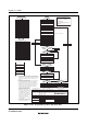
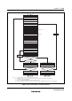
17.16.3 Erase Mode (n = 1 for addresses H'000000 to H'03FFFF, and n = 2 for addresses
H'040000 to H'07FFFF)
Flash memory erasing should be performed block by block following the procedure shown in the
erase/erase-verify flowchart (single-block erase) shown in figure 17.46.
For the wait times (x, y, z, α, ß, γ, ε, η, θ) after bits are set or cleared in flash memory control
register n (FLMCRn) and the maximum number of programming operations (N), see section
20.3.6, Flash Memory Characteristics.
To perform data or program erasure, make a 1 bit setting for the flash memory area to be erased in
erase block register 1 or 2 (EBR1 or EBR2) at least (x) μs after setting the SWEn bit to 1 in flash
memory control register n (FLMCRn). Next, the watchdog timer is set to prevent overerasing in
the event of program runaway, etc. Set a value greater than (y + z + α + ß) ms as the WDT
overflow period. After this, preparation for erase mode (erase setup) is carried out by setting the
ESUn bit in FLMCRn, and after the elapse of (y) μs or more, the operating mode is switched to
erase mode by setting the En bit in FLMCRn. The time during which the En bit is set is the flash
memory erase time. Ensure that the erase time does not exceed (z) ms.
Note: With flash memory erasing, prewriting (setting all data in the memory to be erased to 0) is
not necessary before starting the erase procedure.