
Datasheet


Section 17 ROM
Rev.7.00 Feb. 14, 2007 page 586 of 1108
REJ09B0089-0700
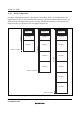
Table 17.7 Flash Memory Erase Blocks
Block (Size) Address
EB0 (4 kbytes) H'000000 to H'000FFF
EB1 (4 kbytes) H'001000 to H'001FFF
EB2 (4 kbytes) H'002000 to H'002FFF
EB3 (4 kbytes) H'003000 to H'003FFF
EB4 (4 kbytes) H'004000 to H'004FFF
EB5 (4 kbytes) H'005000 to H'005FFF
EB6 (4 kbytes) H'006000 to H'006FFF
EB7 (4 kbytes) H'007000 to H'007FFF
EB8 (32 kbytes) H'008000 to H'00FFFF
EB9 (64 kbytes) H'010000 to H'01FFFF
EB10 (64 kbytes)
*
2
H'020000 to H'02FFFF
EB11 (64 kbytes)
*
2
H'030000 to H'03FFFF
EB12 (64 kbytes)
*
1
H'040000 to H'04FFFF
EB13 (64 kbytes)
*
1
H'050000 to H'05FFFF
Notes: 1. These blocks are valid only in the H8S/2315 F-ZTAT and H8S/2314 F-ZTAT.
2. Not available in the H8S/2317 F-ZTAT.
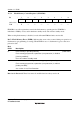
17.5.5 System Control Register 2 (SYSCR2)
Bit : 7 6 5 4 3 2 1 0
— — — — FLSHE — — —
Initial value : 0 0 0 0 0 0 0 0
R/W : — — — — R/W — — —
SYSCR2 is an 8-bit readable/writable register that performs on-chip flash memory control.
SYSCR2 is initialized to H'00 by a reset and in hardware standby mode.
SYSCR2 can only be used in the F-ZTAT versions. In the mask ROM versions this register will
return an undefined value if read, and cannot be modified.
Bits 7 to 4—Reserved: These bits cannot be modified and are always read as 0.