
Datasheet


Section 1 Overview
Rev.7.00 Feb. 14, 2007 page 21 of 1108
REJ09B0089-0700
Pin No.
Type Symbol
TFP-100B,
TFP-100G
FP-100A TLP-113V I/O Name and Function
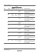
Interrupts NMI 63 65 F8 Input Nonmaskable interrupt: Requests a
nonmaskable interrupt. When this pin
is not used, it should be fixed high.
IRQ7 to
IRQ0
94, 93,
13, 12,
73 to 76
96, 95,
15, 14,
75 to 78
C5, C6, F4,
F1, C10,
B10, B11,
A10
Input Interrupt request 7 to 0: These pins
request a maskable interrupt.
Address
bus
A23 to
A0
2, 1,
100, 99, 53
to 50, 48 to
41, 39 to 32
4 to 1,
55 to 52,
50 to 43,
41 to 34
C1, B1, A2,
B2, J11,
L11, K11,
L10, K9,
J9, K8, K7,
L8, J7, J6,
K6, H7, H6,
L6, K5, J5,
H5, L5, K4
Output Address bus: These pins output an
address.
Data bus D15 to
D0
30 to 19, 17
to 14
32 to 21,
19 to 16
L4, H3, L3,
L1, L2, K1,
K2, J2, J3,
H4, G2,
H1, F3, F2,
G1, G4
I/O Data bus: These pins constitute a
bidirectional data bus.
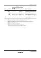
Bus control CS7 to
CS0
94 to 97
75, 76
96 to 99
77, 78
A3, C5,
B11, A10,
A4, B4
Output Chip select: Signals for selecting
areas 7 to 0.
AS 70 72 E10 Output Address strobe: When this pin is low, it
indicates that address output on the
address bus is enabled.
RD 71 73 D8 Output Read: When this pin is low, it indicates
that the external address space can
be read.
HWR 72 74 C11 Output High write: A strobe signal that writes
to external space and indicates that
the upper half (D15 to D8) of the data
bus is enabled.
LWR 73 75 C10 Output Low write: A strobe signal that writes
to external space and indicates that
the lower half (D7 to D0) of the data
bus is enabled.