
Datasheet

Section 8 I/O Ports
Rev.7.00 Feb. 14, 2007 page 284 of 1108
REJ09B0089-0700
8.11.2 Register Configuration
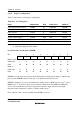
Table 8.19 shows the port F register configuration.
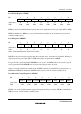
Table 8.19 Port F Registers
Name Abbreviation R/W Initial Value Address
*
1
Port F data direction register PFDDR W H'80/H'00
*
2
H'FEBE
Port F data register PFDR R/W H'00 H'FF6E
Port F register PORTF R Undefined H'FF5E
Bus control register L BCRL R/W H'3C H'FED5
System control register SYSCR R/W H'01 H'FF39
Port function control register 1 PFCR1 R/W H'0F H'FF45
Port function control register 2 PFCR2 R/W H'30 H'FFAC
Notes: 1. Lower 16 bits of the address.
2. Initial value depends on the mode.
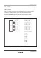
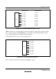
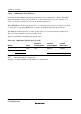
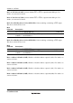
Port F Data Direction Register (PFDDR)
Bit : 7 6 5 4 3 2 1 0
PF7DDR PF6DDR PF5DDR PF4DDR PF3DDR PF2DDR PF1DDR PF0DDR
Modes 4 to 6
*
Initial value : 1 0 0 0 0 0 0 0
R/W : W W W W W W W W
Mode 7
*
Initial value : 0 0 0 0 0 0 0 0
R/W : W W W W W W W W
PFDDR is an 8-bit write-only register, the individual bits of which specify input or output for the
pins of port F. PFDDR cannot be read; if it is, an undefined value will be read.
PFDDR is initialized by a reset, and in hardware standby mode, to H'80 in modes 4 to 6
*
, and to
H'00 in mode 7
*
. It retains its prior state in software standby mode. The OPE bit in SBYCR is
used to select whether the bus control output pins retain their output state or become high-
impedance when a transition is made to software standby mode.
Note: * Modes 6 and 7 are not available in the ROMless versions.