
Datasheet


Section 8 I/O Ports
Rev.7.00 Feb. 14, 2007 page 239 of 1108
REJ09B0089-0700
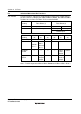
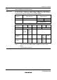
Pin Selection Method and Pin Functions
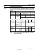
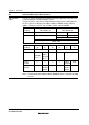
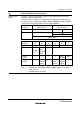
P26/TIOCA5/
TMO0
The pin function is switched as shown below according to the combination of
the TPU channel 5 setting by bits MD3 to MD0 in TMDR5, bits IOA3 to IOA0 in
TIOR5, bits CCLR1 and CCLR0 in TCR5, bits OS3 to OS0 in TCSR0, and bit
P26DDR.
OS3 to OS0 All 0 Any 1
TPU Channel
5 Setting
Table
Below (1)
Table Below (2)
—
P26DDR — 0 1 —
Pin function TIOCA5
output
P26 input P26 output TMO0 output
TIOCA5 input
*
1
TPU Channel
5 Setting
(2)
(1)
(2)
(1)
(1)
(2)
MD3 to MD0 B'0000, B'01×× B'001× B'0010 B'0011
IOA3 to IOA0 B'0000
B'0100
B'1×××
B'0001 to
B'0011
B'0101 to
B'0111
B'××00 Other than B'××00
CCLR1,
CCLR0
— — — — Other
than B'01
B'01
Output
function
— Output
compare
output
— PWM
mode 1
output
*
2
PWM
mode 2
output
—
×: Don’t care
Notes: 1. TIOCA5 input when MD3 to MD0 = B'0000 or B'01×× and IOA3 = 1.
2. TIOCB5 output is disabled.