
Datasheet


Section 20 Electrical Characteristics
Rev.7.00 Feb. 14, 2007 page 833 of 1108
REJ09B0089-0700
(4) Timing of On-Chip Supporting Modules
Table 20.7 Timing of On-Chip Supporting Modules
Condition A: V
CC
= 2.7 V to 3.6 V, AV
CC
= 2.7 V to 3.6 V, V
ref
= 2.7 V to AV
CC
, V
SS
= AV
SS
=
0 V, φ = 2 MHz to 20 MHz, T
a
= –20°C to 75°C (regular specifications),
T
a
= –40°C to 85°C (wide-range specifications)
Condition B: V
CC
= 3.0 V to 3.6 V, AV
CC
= 3.0 V to 3.6 V, V
ref
= 3.0 V to AV
CC
, V
SS
= AV
SS
=
0 V, φ = 2 MHz to 25 MHz, T
a
= –20°C to 75°C (regular specifications),
T
a
= –40°C to 85°C (wide-range specifications)
Condition A Condition B
Item Symbol Min Max Min Max Unit
Test
Conditions
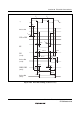
I/O ports Output data delay time t
PWD
— 50 — 40 ns Figure 20.13
Input data setup time t
PRS
30 — 25 — ns
Input data hold time t
PRH
30 — 25 — ns
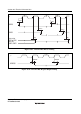
TPU Timer output delay time t
TOCD
— 50 — 40 ns Figure 20.14
Timer input setup time t
TICS
30 — 25 — ns
Timer clock input setup time t
TCKS
30 — 25 — ns Figure 20.15
Single-edge
specification
t
TCKWH
1.5 — 1.5 — t
cyc
Timer clock
pulse width
Both-edge
specification
t
TCKWL
2.5 — 2.5 — t
cyc
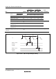
8-bit timer Timer output delay time t
TMOD
— 50 — 40 ns Figure 20.16
Timer reset input setup time t
TMRS
30 — 25 — ns Figure 20.18
Timer clock input setup time t
TMCS
30 — 25 — ns Figure 20.17
Single-edge
specification
t
TMCWH
1.5 — 1.5 — t
cyc
Timer clock
pulse width
Both-edge
specification
t
TMCWL
2.5 — 2.5 — t
cyc
WDT Overflow output delay time t
WOVD
— 50 — 40 ns Figure 20.19