
Datasheet


Section 20 Electrical Characteristics
Rev.7.00 Feb. 14, 2007 page 823 of 1108
REJ09B0089-0700
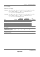
(2) Control Signal Timing
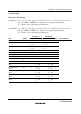
Table 20.5 Control Signal Timing
Condition A: V
CC
= 2.7 V to 3.6 V, AV
CC
= 2.7 V to 3.6 V, V
ref
= 2.7 V to AV
CC
, V
SS
= AV
SS
=
0 V, φ = 2 MHz to 20 MHz, T
a
= –20°C to 75°C (regular specifications),
T
a
= –40°C to 85°C (wide-range specifications)
Condition B: V
CC
= 3.0 V to 3.6 V, AV
CC
= 3.0 V to 3.6 V, V
ref
= 3.0 V to AV
CC
, V
SS
= AV
SS
=
0 V, φ = 2 MHz to 25 MHz, T
a
= –20°C to 75°C (regular specifications),
T
a
= –40°C to 85°C (wide-range specifications)
Condition A Condition B
Item Symbol Min Max Min Max Unit
Test
Conditions
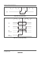
RES setup time t
RESS
200 — 200 — ns
RES pulse width t
RESW
20 — 20 — t
cyc
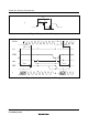
Figure 20.4
NMI setup time t
NMIS
150 — 150 — Figure 20.5
NMI hold time t
NMIH
10 — 10 —
NMI pulse width (in recovery
from software standby mode)
t
NMIW
200 — 200 —
ns
IRQ setup time t
IRQS
150 — 150 — ns
IRQ hold time t
IRQH
10 — 10 —
IRQ pulse width (in recovery
from software standby mode)
t
IRQW
200 — 200 —